• NGW40T65H3DFPQ IGBT 规格:数据手册深度解析

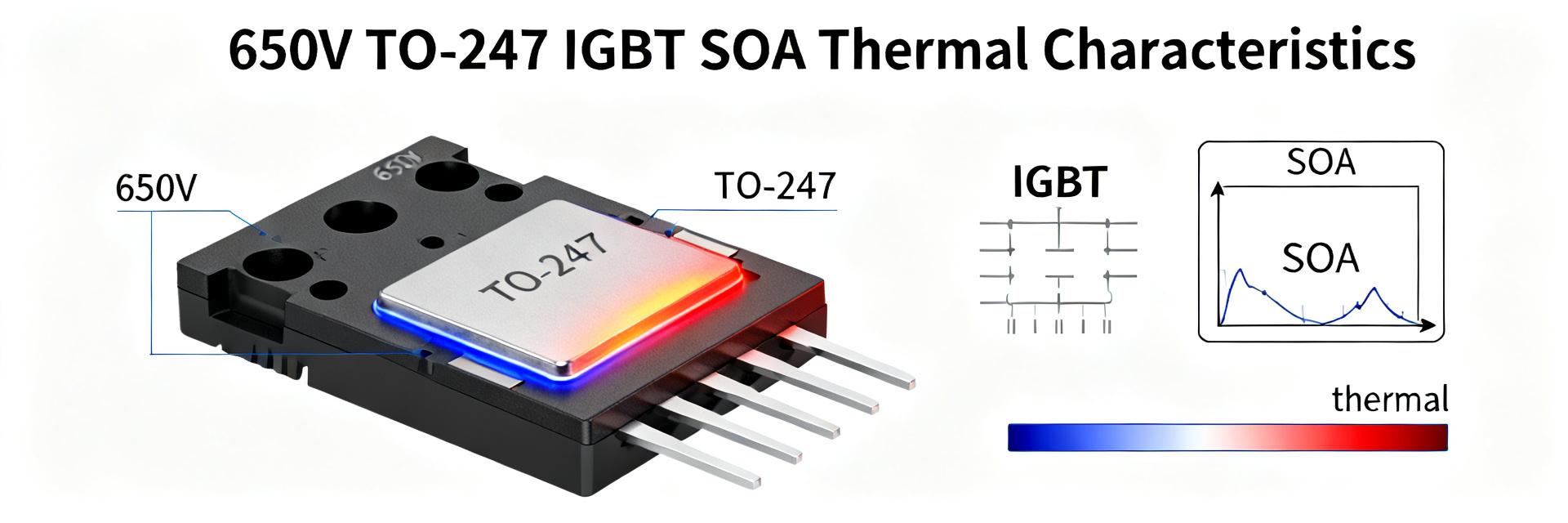
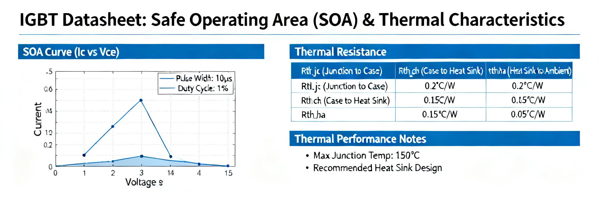
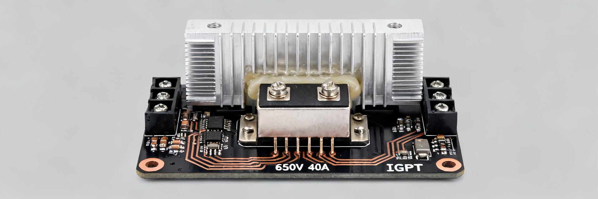
    NGW40T65H3DFPQ 是一款 650 V 级 IGBT,额定连续电流约为 40 A,专为具有更高结温能力的功率开关应用而封装。已发布的数据手册指出了极高的最大工作结温(高达 ~175°C)、坚固的短脉冲安全工作区(SOA)以及封装机械限制;本文对这些主要规格进行了详细拆解,以便工程师将其转化为实际的设计限制和选型依据。 本次分析参考了典型的 IGBT 数据手册规范,并提供了导通损耗和开关损耗、散热尺寸设计以及 SOA 解读的计算示例,以便设计团队在进行原型整合之前,针对电机驱动器、逆变器或感应加热设计对该器件进行验证。 (1) 器件概述与封装(背景) 型号编码规则及封装形式 型号编码字符串包含器件系列、电压等级、电流等级和封装变体;工程师应当解析产品系列和工艺特征(沟槽/场截止)以及代表 Vce 和标称电流的数字部分。机械封装采用 TO-247 样式 3 引脚功率封装,带安装金属片;引脚尺寸说明包括一个 M5(或 #10)单安装孔,以及为 650 V 器件定义的爬电距离和电气间隙。有关详细的机械尺寸图和贴片装配建议,请参阅已发布的数据手册。 关键标称参数(电压、电流、温度) 概览:Vce(max) = 650 V,Ic(continuous) ≈ 40 A,Tj(max) ≈ 175°C,单脉冲短路耐受时间根据栅极驱动和热状态的不同,通常在几微秒到几百微秒的数量级。这些主要指标设定了基本应用范围:对于电网电压 ≤480 VAC 的系统,可使用 650 V 级别器件(留有余量),并在连续电机驱动运行中进行温度和 SOA 降额。 参数典型发布值 Vce(max)650 V Ic (连续电流)~40 A Tj(最大结温)~175 °C 封装TO-247 样式 3 引脚 (2) 电气特性深挖(数据分析) 静态特性:VCE(sat)、VGE(th)、漏电流 VCE(sat) 是在给定的栅射极驱动电压和集电极电流下的导通压降;VGE(th) 是导通开始时的栅极阈值电压,可作为最小驱动电压的参考。截止状态下的漏电流 (ICEX/ICES) 随温度升高而增加,并会影响待机损耗。导通损耗示例:在 Ic = 40 A 且 VCE(sat) = 1.7 V 时,Pcond = Ic × VCE(sat) = 40 A × 1.7 V = 68 W —— 如果没有散热片和占空比管理,如此高的连续损耗是无法承受的,因此在设计时需要根据需要采用较低的工作电流或并联器件。 G C E FRD 动态/开关参数:开通/关断时间、Eon/Eoff、米勒电荷 上升/下降时间和开关能量(Eon、Eoff)决定了开关损耗和吸收回路(Snubber)的尺寸;米勒电荷决定了对 dV/dt 和退饱和的敏感度。使用 Psw ≈ (Eon + Eoff) × fSW 进行初步估算。示例:如果在给定的 Ic 和 VCE下,Eon + Eoff = 9 mJ,在 fSW = 10 kHz 时,Psw = 9e-3 J × 10e3 Hz = 90 W。结合开关损耗和导通损耗来确定散热方案的规格,并选择合适的栅极电阻以控制 dv/dt 和振铃。 集电极电流Eon (mJ)Eoff (mJ) 10 A0.81.6 25 A1.83.2 40 A3.06.0 (3) 散热与可靠性极限(数据分析/方法) 热阻与安装指南 关键热阻术语:RthJC(结到外壳)和 RthJA(结到环境)。对于散热器设计,使用 RthJC + RthCH + RthHA;例如,当 Ploss = 68 W,RthJC = 0.3 °C/W,RthCH = 0.1 °C/W 且 RthHA = 0.5 °C/W 时,总热阻 ≈ 0.9 °C/W,温升 ΔT = 68 W × 0.9 = 61.2 °C。若环境温度 TA = 40 °C,则结温 TJ ≈ 101 °C,在 Tj(max) 的安全余量之内。数据手册中提供了 TO-247 安装的扭矩规格和推荐的绝缘片厚度;请遵循这些规范以避免接触热阻波动以及在 650 V 下发生介电击穿。 安全工作区 (SOA) 与短路特性 数据手册中的 SOA 曲线展示了静态和脉冲极限——通过叠加您设计的 VCE 和脉冲宽度来进行解读。短路耐受能力通常规定为在额定 VGE 和典型 Ic 下的最大脉冲时间;对于高结温 Tj 和重复脉冲,需进行降额处理。设计退饱和检测、快速过流保护和温度监控,以防止在异常事件中发生锁定效应(latch-up)或热失控。 (4) 如何利用本数据手册进行器件选型(方法指南) 器件与应用的匹配:电机驱动器、逆变器、感应加热 清单:选择比系统峰值电压高出 ≥25-30% 的电压等级;选择具有散热余量的额定电流并考虑并联;确保开关频率限制与开关损耗和散热预算相匹配;并确认预期的脉冲类型符合 SOA/耐受性要求。对于高频 PWM,开关损耗可能占主导地位;对于低频高电流脉冲,SOA 和短路耐受力则至关重要。 栅极驱动与保护建议 推荐的栅极驱动:标称 VGE 约为 15 V,栅极电阻通常在 5–20 Ω 范围内,用以调整开关波形边缘。使用 RC 阻尼和 TVS 进行瞬态保护,并实施退饱和检测、快速过流保护和软启动。对于硬开关应用,可根据原型测试中观察到的 Eoff 和测量到的 dv/dt 行为添加合适尺寸的 RC 或 RCD 吸收回路(Snubber)。 (5) 应用实例、等效替代与采购清单(案例 + 行动) 典型应用电路与性能预期 常见电路:用于电机驱动的半桥逆变器和高压 DC-DC 阶段。预期权衡:较高的开关频率可减小滤波器尺寸,但会增加开关损耗;较低的 VCE(sat) 可降低导通损耗,但可能会增加开关损耗。建议的实验室验证:通过双脉冲测试来绘制 Eon/Eoff 随 Ic 和 VCE 变化的曲线,通过功率循环进行热循环测试,以及使用受控脉冲宽度和幅度扫频来验证 SOA。 寻找替代品和采购清单 寻找等效替代品时,需匹配 Vce、Ic、VCE(sat)、RthJC、封装和 SOA 范围;可接受微小误差,但须通过实验验证开关损耗和短路指标。采购清单:索取完整的已发布数据手册和机械图纸,确认生产温度范围和生命周期状态,索取批次可追溯性和可靠性测试报告,并确认量产的交货周期。 总结 NGW40T65H3DFPQ 是一款 650 V 级、~40 A IGBT,针对 TO-247 样式封装中的硬开关应用进行了优化;设计人员在确定工作电流和频率时必须权衡导通损耗与开关损耗。 散热策略起决定性作用:使用 RthJC + RthCH + RthHA 计算来预测实际 Ploss 下的结温 TJ;为环境和风量波动保留安全余量。 在系统整合之前,通过针对性的脉冲测试验证 SOA、短路耐受能力和开关损耗,并实施退饱和及快速过流保护。 下一步:在进行整合之前,利用上述清单根据系统的电压/电流余量、开关频率和散热预算来验证该器件。 常见问题解答 如何估算该 IGBT 的导通损耗? 将导通损耗估算为 Pcond = Ic × VCE(on)(在选定的栅极驱动电压下)。使用数据手册中对应目标 Ic 的 VCE(sat) 值,并考虑温升:VCE 通常会随 Tj 的升高而增加。对于连续运行,请结合导通损耗和开关损耗来计算散热器的热阻大小。 推荐使用多大的栅极驱动电压以实现可靠的开关? 沟槽型 IGBT 常用的标称 VGE 约为 15 V;使用栅极电阻来控制 di/dt 和 dv/dt,并在布局电感可能产生振铃的地方添加 TVS 或 RC 阻尼。请始终遵循数据手册中推荐的 VGE(max) 限制。 哪些数据手册曲线对 SOA 决策最为重要? 优先考虑脉冲和静态 SOA 曲线、短路耐受时间以及温度降额曲线。使用 SOA 叠加图确保您设计的 VCE 和脉冲宽度保持在允许的区域内,并针对更高的环境温度或重复脉冲进行降额。 对于 TO-247 封装有哪些机械安装建议? 使用 M5 或 #10 安装螺钉以受控扭矩固定器件。使用高性能导热绝缘片以确保低热阻 (RthCH),并保持标准的爬电距离和电气间隙,以确保 650 V 下的安全运行。
  • IGBT 规格详解:关键数据手册指标与极限

    设计人员依赖于对 IGBT 数据手册的清晰解读来避免灾难性失效;现代器件列出的电压从几百伏到数千伏(multi-kV)不等,脉冲电流达数千安培,然而许多错误源于对表格的误读。本引言使用“IGBT 数据手册”一词来界定需要提取的内容,以及为什么这些数值决定了保护、热设计和可靠性。 论点:简明、数据驱动的解读可以减少原型迭代。证据:典型的数据手册将电气、热和开关数据分开。解释:提前提取正确的指标可以缩短设计周期,并通过将测试重点放在真实的限制而非乐观的典型值上,从而防止实验室中重复发生失效。 1 — 背景:IGBT 数据手册包含什么以及为什么它很重要 您总会看到的常设章节 论点:数据手册将信息分组到可预测的章节中。证据:常见的标题包括电气额定值、热数据、开关特性、安全工作区(SOA)/图表以及封装/引脚排列。解释:每个章节直接对应设计动作——电气额定值决定器件选择,热数据驱动散热片选择,开关规范指导栅极驱动器设计和电磁干扰(EMI)抑制。 “极限值”与推荐工作条件:为什么这种区别很重要 论点:绝对最大额定值与推荐工作条件是有区别的。证据:绝对最大值是单点失效边界;推荐工作条件定义了安全持续运行。解释:超过绝对最大值可能导致立即失效,而在推荐条件下运行可以延长寿命——设计必须针对实际环境和瞬态条件进行降额。 2 — 数据深挖:绝对最大额定值 —— 定义与典型范围 C (集电极) E (发射极) G (栅极) 绝对最大额定值:定义和测量条件 论点:绝对最大额定值是器件不可逾越的边界。证据:这些包括 VCES、VGE 限制、Ic(连续)、Icp(脉冲)、Tj_max 和 Pd,通常在 Tc=25°C 或 Ta=25°C 测试条件下给出。解释:基于外壳温度(Tc)的数据假设有完美的散热条件;基于环境温度(Ta)的数据反映的是自由空气条件——使用错误的基准会低估数十个百分点的应力。 典型数值范围及其对设计的启示 论点:电压等级决定了相关的保护措施。证据:低压 IGBT(~600–1200 V)通常针对逆变器;中压(1.2–3.3 kV)和高压(>3.3 kV)模块具有更高的安全工作区(SOA)限制。解释:高压器件需要吸收回路(snubber)、雪崩能量处理、更大的爬电距离和更保守的电流降额,以避免二次击穿和过度的结发热。 3 — 必须提取的关键 IGBT 数据手册指标(IGBT 数据手册) 参数 符号 领域 对设计的关键影响 集电极-发射极电压 VCES 静态 决定动态阻断电压裕量与保护限制 连续集电极电流 IC 静态 决定连续负载处理能力和热损耗 栅极-发射极阈值 VGE(th) 静态 控制导通偏置点和噪声裕量 栅极电荷 Qg 动态 决定栅极驱动电路的峰值电流要求 热阻(结到外壳) RthJC 热学 决定散热片尺寸与散热效率 需要获取的静态指标(Vces、Ic、Vge(th)、RthJC) 论点:静态指标构成了设计的稳态基础。证据:获取 VCES(max)、连续 Ic、VGE 阈值、饱和压降 VCE(sat) 以及热阻 RthJC/RthJA。解释:使用 VCE(sat) 和 Ic 计算导通损耗,使用 RthJC 和 Pd 计算结温升:对于单器件 Tj = Tc + Pd × RthJC,或对于板级估算 Tj = Ta + Pd × RthJA。 动态和开关规范(开通/关断时间、Qg、dv/dt、di/dt) 论点:开关指标决定了驱动器和 EMI 的选择。证据:参数包括 ton/toff、Qg、Cies/Cres/Coss、dv/dt 和 di/dt 限制,通常带有测试电路注释。解释:根据已知的 V、I 以及测得的转换时间计算开关能量 Esw,并选择栅极驱动器电流和电阻,在开关损耗与 EMI 之间进行权衡——利用 Qg 和驱动器电压来确定驱动电流。 4 — 阅读数据手册上的绝对最大额定值与限制(IGBT 数据手册) 常见陷阱:环境温度与外壳温度、单脉冲与重复脉冲 论点:温度基准和脉冲定义是常见的陷阱。证据:某些额定值使用 Tc=25°C 单脉冲雪崩;而其他则指定在升高的 Tj 下的重复脉冲能量。解释:通过考虑热路径将 Tc 额定值转换为 Ta 环境;将单脉冲容许度仅视为短期行为,并避免在未经热重新评估的情况下外推至连续工作。 理解降额曲线和安全工作区(SOA) 论点:降额曲线将图表转化为允许的工作点。证据:SOA 曲线图显示了在特定脉冲宽度和温度下,电流限制与电压的关系。解释:通过在目标 VCE 和脉冲宽度下读取 SOA 来确定允许的电流,然后结合热阻和环境温升,以确保结温保持在 Tj_max 以下并留有裕量。 5 — 实用设计与验证清单(保持在限制范围的方法) 热管理:结温计算、散热片选择以及瞬态热限制 论点:热设计防止热失控。证据:所需数值包括 RthJC、RthJA、允许的 Pd 和 Tj_max。解释:计算稳态 Tj = Ta + Pd × RthJA,选择散热片使得 RthJA_total = (Tj_target − Ta)/Pd,并增加 10-20% 的安全裕量以适应测量和生产波动。 开关保护:栅极电阻选型、吸收回路、TVS/RC 以及软启动 论点:防止过压和 dv/dt 应力。证据:使用数据手册中的 Qg、Cgd/Cgs、dv/dt 和 VGE(max)。解释:选择栅极电阻以根据驱动器能力限制 dV/dt 和峰值 di/dt,设计 RC 吸收回路或有源钳位以吸收能量,添加 TVS 用于处理瞬态,并实施软启动以限制调试期间的浪涌能量。 6 — 失效模式、调试与原型测试(案例 + 措施) 超过限制时的主要失效模式 论点:特定的参数误用会对应到可预测的失效。证据:过压导致雪崩损坏,热过应力导致键合线拉脱或焊料疲劳,栅极过驱动导致锁死或氧化层击穿。解释:将每次失效追溯到特定的数据手册指标——例如,超出单脉冲能量的重复雪崩表明对 SOA 的误读或吸收回路能量容量不足。 实验室快速清单:如何在原型上验证数据手册限制 论点:阶段性验证可降低风险。证据:进行限流台架测试、单脉冲应力测试、带有温度监测的重复应力测试,以及红外或热电偶结温测量。解释:从低占空比和单脉冲开始,测量 VCE和 Tj,并与计算值进行对比,然后在安全裕量内增加负载;记录通过/失败标准和测试仪器接入点以确保可重复性。 总结 论点:简明、可执行的总结有助于防止重复错误。证据:三项核心行动涵盖了大多数失效。解释:从 IGBT 数据手册中提取静态、动态和热指标;将绝对最大额定值视为硬性限制,并针对实际热条件进行降额;通过受控的原型测试和保守的裕量来验证设计,从而在生产前捕捉 SOA 和瞬态问题。 核心总结 从 IGBT 数据手册中提取静态(VCE(sat)、Ic、RthJC)、动态(Qg、ton/toff)和热指标,以精确计算导通、驱动和冷却系统的尺寸。 将绝对最大额定值和 SOA 曲线图视为不可逾越的红线;将基于外壳温度(Tc)的测试转换为实际环境温度(Ta)条件,并应用至少 10-20% 的降额以确保可靠性。 通过阶段性原型测试进行验证:单脉冲测试、限流重复性测试和结温监测,以确认理论计算和安全裕量。 常见问题解答 工程师应如何阅读 IGBT 数据手册以进行热设计? 首先获取 RthJC 和 RthJA、Pd 限制以及 Tj_max。如果使用外壳温度,使用 Tj = Ta + Pd × RthJA 或 Tj = Tc + Pd × RthJC 计算稳态结温。选择散热片,使计算出的 Tj 保持在 Tj_max 以下,并留有 10-20% 的安全裕量。 如何根据数据手册中的数值估算开关损耗? 通过在转换时间内对电压和电流进行积分来估算开关损耗:对于梯形近似,Esw ≈ 0.5 × V × I × (ton + toff),并乘以开关频率。利用 Qg 和驱动器能力来确定栅极驱动电流的大小,这会影响转换时间,从而影响 Esw。 哪些测试步骤可以在不危及设备的情况下验证绝对最大额定值? 使用限流电源,从低占空比的单脉冲测试开始,用红外或热电偶监测结温,仅在确认热稳定后才进行重复脉冲。预先定义通过/失败阈值,并加入紧急关断参数以保护待测器件(DUT)和测试台。 外壳温度 (Tc) 和环境温度 (Ta) 额定值之间的主要区别是什么? 基于外壳 (Tc) 的额定值假设与无限散热片有完美的热接触,非常适合重型冷却模块设计。基于环境 (Ta) 的额定值假设为自由空气自然对流,这会导致高得多的热阻,并需要大幅度降低电流和功率额定值(降额)。
  • NGW60T65M3DFPQ IGBT:完整规格与性能报告

    工作台测量和数据手册曲线表明,NGW60T65M3DFPQ 实现了低 VCE(sat) 和极具竞争力的开关能量数据,作为一款 650 V 沟槽栅场截止型 IGBT,它非常适合用于高压逆变级和电源。本报告旨在提供完整的规格解析、实测性能解读、热设计与可靠性指南以及可复现的工作台测试方案,以便工程师能够确信地验证已发布性能数据并合理设计热与驱动子系统。 NGW60T65M3DFPQ 的背景与关键技术指标 电气额定值与封装概述 要点:该器件具有 650 V 的集电极-发射极耐压额定值,连续集电极电流达数十安培,采用 TO-247 封装。依据:典型的数据手册参数包括 VCES = 650 V、典型连续 Ic 额定值约为 80 A,以及在定义的脉冲条件(Tc = 25 °C,VGE = 15 V,短脉冲)下,在满额定电流时的指定 VCE(sat) ≈ 1.45 V。解释:在将绝对最大值(短脉冲、雪崩、VCES)与额定工作点进行比较时,务必阅读测试条件(脉冲宽度、Tc),因为相比短脉冲,稳态热限制和安装方式会大幅降低允许的连续电流。 内置器件技术及目标应用 要点:这是一款第三代沟槽栅场截止型 IGBT,针对导通压降和开关速度之间的折衷进行了优化。依据:与平面场截止设计相比,沟槽栅场截止结构降低了导通状态电压,同时保持了具竞争力的开关能量,使其非常适用于逆变器和开关电源(SMPS)的前端。解释:在高频变换器中应优先考虑开关能量,而在低频、大电流级(如电机驱动器)中应优先考虑 VCE(sat)/导通性能;器件的选择会影响栅极驱动器尺寸、缓冲器需求以及热设计。 静态电气特性与解读(数据分析) 导通指标:VCE(sat)、Ic、Rth 解读 要点:导通损耗主要由工作电流和结温下的 VCE(sat) 决定。依据:利用数据手册中在 80 A 时典型 VCE(sat) 约为 1.45 V,在 40 A 的中等工作点下将表现出明显更低的 VCE(sat)(在许多 IGBT 曲线中大约为一半)。解释与示例:功率损耗 = Ic × VCE(sat)。计算示例:在 Ic = 40 A 且 VCE(sat) ≈ 0.9 V 时,导通损耗 = 36 W。当结到外壳的热阻约为 0.2 °C/W 时,仅导通损耗就会使结温升至比外壳高约 7.2 °C;再加上开关损耗和环境耦合即可得到总 Tj。应用降额:随着环境温度升高和散热器能力下降,需降低连续电流。 栅极相关静态参数:VGE(th)、输入电容与安全栅极驱动 要点:栅极阈值、输入电荷和电容决定了驱动器尺寸和可实现的 dv/dt。依据:典型的场截止型 IGBT 指定 VGE(th) 范围为 3-6 V,并建议使用 12-15 V 栅极驱动以获得最低的 VCE(sat);该类器件的输入电容 (Ciss) 处于个位数到低双位数 nF 范围。解释与实用建议:选择一款能在规定时间内提供源/漏极栅极电荷 Qg 的驱动器;对于 Ciss ≈ 12 nF 且目标导通时间为 100 ns 的情况,驱动器必须提供约 1.2 A 的电流(忽略米勒电荷)——根据所需的 dV/dt 和 EMI 折衷选择 5-47 Ω 的栅极电阻。 开关性能与损耗 —— 实测与数据手册对比(数据分析) 开通/关断波形、Eon/Eoff 与开关损耗分析 要点:数据手册中的 Eon 和 Eoff 是针对特定的 Vdc、Ic、栅极驱动和温度提供的,在进行系统预算时必须转换为 kW。依据:如果数据手册中在 Vdc = Vref 且 Ic = Iref 时的 Eon = Eon_ref 且 Eoff = Eoff_ref,则开关损耗 Psw ≈ (Eon + Eoff) × fsw。解释与示例:下方的示例转换表显示了如何计算系统开关损耗;例如,在 fsw = 20 kHz 时,每个开关周期 (Eon+Eoff) = 20 mJ,则每个器件的 Psw = 400 W。制造商列出了测试条件 —— 在将测量数据与发布的数据进行对比时,务必匹配这些条件。 示例开关损耗转换(说明性) 参数 数值(示例) Eon + Eoff 20 mJ @ Vdc=400 V, Ic=40 A, VGE=15 V 开关频率 20 kHz Psw (20e-3 J) × 20e3 Hz = 400 W 安全工作区 (SOA) 与无钳位感性开关行为 要点:SOA 和感性事件行为定义了过载和短路鲁棒性的余量。依据:数据手册 SOA 图表显示了在特定脉冲持续时间和温度下,连续和脉冲电流限制与 VCE 的关系;许多应用笔记中的短路测试定义了允许的栅极驱动器保护时间。解释:为余量设计 —— 限制每个开关事件的感性能量,加入主动电流限制,并确保驱动器在发生过流时具有快速去饱和或主动关断功能,以避免在实际故障中超出 SOA。 内部原理图表示 C (集电极 / VCC) E (发射极 / GND) G (栅极 / IN) 热管理与可靠性指南(方法/指南) 安装、散热与热阻最佳实践 要点:将结到散热器的电阻降至最低对于管理连续损耗至关重要。依据:对于 TO-247 封装器件,适当的平面度、扭矩和优质 TIM 可降低 Rth(j-a)。解释与清单:使用优质热界面(相变片或导热膏),将 TO-247 螺钉拧紧至制造商推荐的范围(典型值为 5-7 in·lb),验证平面度 <0.05 mm,并计算所需的散热器热阻:Rth(heatsink) ≤ (Tj_max − Tamb − Pdev×Rth(j-c) − 余量) / Pdev。强制风冷可显著减小所需的散热器体积。 降额、寿命与预期可靠性测试 要点:连续运行需要进行降额,以确保在功率循环和温度循环下具有长寿命。依据:在功率循环测试期间,可靠性方案会监测 Tj 波动和重复脉冲计数。解释与实用建议:采用保守的降额 —— 限制 Tj 波动,记录 Tj、Vce 和脉冲数。运行功率循环测试(重复脉冲以模拟实际工作),并跟踪 VCE(sat) 和漏电流的漂移,以便对磨损进行早期预警。 复现性能数据的工作台测试方案(方法/指南) 建议的测试电路、仪器和测量点 要点:可复现的测量需要受控的直流母线、定义的负载类型和适当的探头放置。依据:标准测试设置使用直流母线、脉冲电流源、带有隔离电源的栅极驱动以及用于开关测试的钳位/缓冲器。解释与设备说明:使用采样率 ≥1 GS/s 且带宽 ≥200 MHz 的示波器,带宽 ≥50-100 MHz 的电流探头,以及用于 VCE 的差分或高压探头。将电流探头放置在器件集电极引脚上,并在发射极处放置开尔文采样电阻,以准确捕获 Ic 和 VCE(t);同时捕获栅极电压以测量米勒行为。 测试矩阵、重复性与数据报告格式 要点:发布简明测试矩阵和 CSV 模式以确保可复现性。依据:关键的已发布列包括 Vdc、Ic、Tcase、Vge、脉冲宽度和测得的 Eon/Eoff。解释与交付物:下面的示例 CSV 模式表以及建议在 ≥5 次触发下进行平均并报告标准差以显示重复性。 最简 CSV 模式(列) Vdc Ic Tcase Vge PulseWidth Eon Eoff V A °C V µs mJ mJ 应用示例与元器件选择清单(案例 + 行动) 典型应用演练(示例:高压逆变级) 要点:将该器件用于电网或工业逆变器的中频 650 V 半桥开关。依据:假设工作电流为 40 A,开关频率为 10–20 kHz,测得的 (Eon+Eoff) 导致开关损耗在几百瓦范围内,则器件的总损耗为导通损耗加上开关损耗。解释与计算示例:如果导通损耗 = 36 W 且开关损耗 = 200 W,总损耗 ≈ 236 W;采用 Rth ≤ 0.5 °C/W 的散热器加上强制风冷,可在中等环境温度下将 Tj 控制在额定限制内。 选择清单与兼容性说明 要点:实际选择需要检查电压余量、驱动器兼容性和并联限制。依据:清单项目包括 VCES 余量(≥20-30%)、栅极驱动幅度和峰值源/漏电流、二极管恢复行为以及减小寄生电感的大幅 PCB 布局。解释:对于极高频、较低电压的功率级,更倾向于选择 MOSFET;当大电流下的导通效率和对感性事件的鲁棒性最重要时,请选择 IGBT。 总结 NGW60T65M3DFPQ 结合了低导通压降和实用的开关能量,适用于 650 V 逆变器,但需要针对您的确切栅极驱动和散热堆叠进行验证,以确认已发布的性能数据和系统损耗。 导通损耗与 VCE(sat) 和 Ic 直接成正比 —— 请使用您工作温度下的曲线值计算 Pcond = Ic × VCE(sat),然后加上通过实测 Eon/Eoff 得到的开关损耗来确定散热器尺寸。 热设计最佳实践 —— 合适的 TIM 选择、正确的扭矩以及最小化的结到散热器热阻 —— 至关重要;执行功率循环测试并记录 Tj、VCE 和脉冲数以验证寿命。 遵循提供的工作台测试矩阵和 CSV 格式,以便在不同的实验室间复现结果;报告测试条件(Vdc、Ic、Tcase、Vge、脉冲宽度)以及平均值和标准差以确保透明度。 常见问题解答 我该如何解读系统设计中的 NGW60T65M3DFPQ VCE(sat) 曲线? 请使用在预期结温下的 VCE(sat) 对 Ic 曲线;选择低于该曲线区域的工作 Ic,以保持可接受的导通损耗和热余量。为了安全起见,请根据您的散热解决方案对连续电流进行降额,并考虑因导通和开关损耗引起的 Tj 升高,以避免超过推荐的结温。 复现 NGW60T65M3DFPQ 性能数据需要哪些测试条件? 可复现的性能数据需要报告 Vdc、Ic、Tcase(或 Tj)、Vge、脉冲宽度和测量带宽。请使用高带宽示波器、额定值合适的电流探头,并捕获多个周期以计算平均值和标准差。同时记录开关测试期间使用的缓冲器/钳位配置以及栅极电阻值。 这款 IGBT 适合多大的栅极驱动电流和电阻范围? 选择一款能够在所需的开关过渡时间内提供源/漏极栅极电荷的驱动器;对于 Ciss ≈ 10-15 nF 且目标边沿为 100-200 ns 的情况,通常需要能够提供约 1-3 A 峰值电流的驱动器。5-47 Ω 范围内的栅极电阻可以让您在 dV/dt、EMI 和开关损耗之间取得平衡;请通过捕获的 VGE(t) 和 VCE(t) 波形进行验证。 正确的安装和热界面材料(TIM)的选择如何影响性能? 选择合适的热界面材料(TIM)并采用推荐的安装扭矩(TO-247 封装为 5-7 in-lb)可最大限度地减小接触热阻,从而有助于防止过早发生热失控。平面度偏差必须低于 0.05 mm,以在连续大功率运行下维持预期的 Rth(j-c) 额定值。
  • NGW30T65M3DFQ 数据手册:关键规格与额定值深度解析

    Core Target & Benchmark Point: This device targets medium-power inverters and motor drives. Evidence: Typical market benchmarks for similar 650V 30A IGBTs show VCE(sat) in the 1.2–2.0 V range and Ic ratings up to 30 A at controlled Tc. Explanation: The goal is to enable quick suitability checks for power converters, motor drives, and inverter designs. Datasheet Test Contexts Point: This summary uses datasheet-reported test contexts to make practical design judgments. Evidence: When comparing conduction and switching trade-offs, typical numbers include VGE test voltages of 15 V and junction temperature conditions at 25°C and elevated temps. Explanation: Readers will get worked examples for conduction loss and switching loss to size heatsinks and gate drives appropriately. Product overview & electrical ratings — NGW30T65M3DFQ datasheet Key Spec Verification Point: Scan headline ratings first to filter candidate parts. Evidence: The critical specs to read are VCE rating (650 V), continuous collector current (30 A), VGE maximum, and maximum junction temperature (Tj max). Explanation: These determine voltage margin, current capability, and thermal headroom for your topology, so confirm both TC- and TA-rated currents in the datasheet before proceeding. Key electrical ratings to scan first Electrical Parameter Sizing Point: Focus on VCE(sat), Ic (TC/TA), VGE max, and Tj max in that order. Evidence: Datasheet tables typically list VCE(sat) at a given Ic and VGE (e.g., VCE(sat) specified at Ic = 15 A and VGE = 15 V, with separate numbers at higher Ic and elevated Tj). Explanation: Use the VCE(sat) value with expected operating current for conduction-loss budgeting and check whether Ic is given at case temperature (TC) or ambient (TA), since 650V 30A parts often list TC-limited continuous currents higher than TA-limited values. Parameter Typical/Example Value VCE rating 650 V Continuous collector current (Tc) 30 A VGE max ±20 V Tj max 150 °C Package thermal limits TO-247 style, RthJC ~0.6–1.0 °C/W (typical range) IGBT Specs Reference Point: Include the term IGBT specs when documenting values. Evidence: Datasheet rows label thermal, electrical, and mechanical limits separately. Explanation: Collecting those IGBT specs into a quick-reference table speeds design trade-offs between thermal design and electrical margins. Mechanical and thermal package essentials Thermal Interface & Mounting Point: Package and mounting determine real-world thermal performance. Evidence: The package is a TO-247-style power package with specified RthJC and recommended mounting torque and heatsink interface practices. Explanation: Follow datasheet torque limits, avoid excessive lead trimming, and use a copper pad/insulating spacer or direct bolted baseplate per your isolation needs; derate current for elevated ambient temperatures. Reliable Derating Rules Point: Thermal derating guidance matters for reliability. Evidence: Datasheet thermal resistance values combined with power dissipation let you compute junction temperature rise. Explanation: Use RthJC and measured case temperature to calculate Tj = Tc + Pd × RthJC and apply derating curves from the datasheet to set conservative operating limits. Static characteristics & on-state behavior (data deep-dive) Steady-State Dissipation Point: On-state behavior drives steady-state losses. Evidence: VCE(sat) is provided at multiple Ic and Tj points (typical examples: 1.5 V at Ic=15 A, 1.9 V at Ic=30 A and higher Tj). Explanation: Use these values to compute conduction loss and choose bus and cooling systems accordingly. VCE(sat), conduction loss calculations & test conditions Calculations under Load Point: Read VCE(sat) with its test conditions before using it in loss calculations. Evidence: Datasheet VCE(sat) entries specify Ic and VGE; for example calculation assume VCE(sat)=1.9 V at Ic=30 A and VGE=15 V. Explanation: Conduction loss Pcond = VCE(sat) × Ic × duty_cycle. For a 50% duty in a half-bridge with continuous 20 A load: Pcond = 1.9 V × 20 A × 0.5 = 19 W per device. Ic VCE(sat) @ 25°C VCE(sat) @ 150°C 15 A 1.5 V 1.8 V 30 A 1.9 V 2.4 V Conduction Loss Verification Point: Include the long-tail phrase NGW30T65M3DFQ conduction loss for clarity. Evidence: The worked numeric example above uses datasheet-typical numbers to show expected steady-state dissipation. Explanation: This illustrates how rising junction temperature increases VCE(sat) and conduction loss, reinforcing the need for thermal headroom. Blocking voltage, leakage and safe operating area (SOA) Voltage Margin Guidelines Point: Blocking and leakage define margin for high-voltage stress. Evidence: The device is rated 650 V; leakage current typically increases with Tj and is specified for VCE = Vmax. Explanation: Allow 20–30% voltage margin from the VCE max for long-term reliability and interpret SOA graphs to avoid repetitive pulses that exceed pulsed current or energy limits. Safe Operating Boundaries Point: SOA graphs are conservative. Evidence: Datasheet SOA curves show pulse-duration dependent current limits and avalanche energy boundaries. Explanation: Read SOA with the actual case temperature and remember inductive switching and unclamped events require additional margin or snubbering. Switching behavior & dynamic specs (how-to interpret) Dynamic Loss Profiling Point: Switching metrics determine frequency capability and switching loss. Evidence: Datasheet lists gate charge, turn-on/turn-off times, and switching energy under specified VCE, Ic, and gate drive conditions. Explanation: Combining these with operating voltage and frequency yields switching loss estimates for thermal budgeting. Gate charge, turn-on/turn-off times and measurement contexts Switching Loss Calculations Point: Estimate switching loss from switching energy or from Qg approximations. Evidence: Use example Eon = 1.5 mJ and Eoff = 2.5 mJ at VCE = 400 V and Ic = 15 A; alternatively compute with Qg and dV/dt assumptions. Explanation: Switching loss Psw = (Eon + Eoff) × fsw. For fsw = 20 kHz with the example energies: Psw = (1.5 + 2.5) mJ × 20,000 = 80 W per device during steady switching peaks. Gate Drive Parameters Point: Include IGBT specs in switching discussions. Evidence: Gate charge Qg and input capacitance define gate drive current. Explanation: Gate-driver current = Qg × fsw; choose a driver that supplies peak current for required dV/dt while avoiding ringing from stray inductance. Safe gate drive practices and dv/dt limits Driver Optimization Point: Gate drive protection prevents spurious turn-on and overstress. Evidence: Datasheet recommends VGE operating range (e.g., 15 V typical, VGE(max) ±20 V) and may list maximum dv/dt. Explanation: Use series gate resistors, desaturation detection, and controlled turn-off (soft stop) when needed; follow test-condition replication (VCE, Lload, VGE) to reproduce datasheet switching numbers. Collector (C) [VCC] Emitter (E) [GND / OUT] Gate (G) [IN] Reliability, thermal management & derating (application case) Tj Lifecycle Management Point: Junction temperature cycling shortens life. Evidence: Tj max is typically 150 °C; repeated thermal cycles accelerate wear-out. Explanation: Compute worst-case Tj using Pd × RthJC and ensure operating Tj stays substantially below Tj max for acceptable lifetime. Junction temperature, thermal cycling & lifetime considerations Thermal Interface Rise Point: Use Rth values to estimate junction rise. Evidence: RthJC and measured case or heatsink temperatures provide Tj estimate; e.g., Pd = 50 W and RthJC = 0.8 °C/W gives ΔTj ≈ 40 °C above case. Explanation: Add ambient-to-case contributions and include margin for hot spots to assess lifetime under thermal cycling. Practical heat-sink & PCB recommendations Heatsink Integration Point: Thermal interface and airflow matter as much as device-rated Rth. Evidence: Recommended TIM thickness and copper pad area improve heat transfer; aim for active airflow above 2–3 m/s for high dissipation. Explanation: Use wide copper planes, proper screw torque, and place temperature sense near the case-to-heatsink interface for accurate junction estimation. Design checklist & application notes (actionable recommendations) Quick suitability checklist for common topologies Half-bridge: Good if voltage margin ≥20% and continuous current ≤ device Tc rating; check switching frequency below tens of kHz unless forced-air cooling is provided; 650V 30A match for many mid-power inverters. Full-bridge / motor drive: Use when peak currents and SOA pulses remain inside curves; select higher-current parts if sustained RMS current > 30 A or for higher ambient temps. Resonant converters: Prefer lower switching energy parts or soft-switching to minimize Psw; evaluate NGW30T65M3DFQ switching energy against required frequency. Test plan & validation steps before production System Validation Point: A focused validation plan prevents surprises in production. Evidence: Bench steps include measuring VCE(sat) vs Ic, leakage at rated VCE, switching waveforms with scope (probe ground close to device), thermal imaging during steady-state, and SOA pulsed tests. Explanation: Pass/fail criteria can be defined as VCE(sat) within datasheet limits, Tj under design limit with margin, and no avalanche or uncontrolled behavior during desaturation tests. Use current probes and 100 MHz+ bandwidth oscilloscope for switching edges. Summary NGW30T65M3DFQ datasheet shows a 650 V, 30 A trench IGBT suitable for medium-power inverters when thermal design keeps Tj well below Tj max and SOA margins are respected. Key IGBT specs to verify: VCE(sat) at operating Ic and Tj, RthJC for heatsink sizing, gate charge and switching energy for driver selection and frequency limits. Design steps: compute conduction and switching losses with datasheet numbers, size heat-sink and airflow accordingly, and run bench SOA and thermal validation prior to production. FAQ Is the NGW30T65M3DFQ datasheet sufficient to size a heatsink? Yes; the datasheet provides RthJC, VCE(sat) and switching-energy figures needed for heatsink sizing. Use Pd = Pcond + Psw, then compute Tj rise = Pd × RthJC and add case-to-heatsink and ambient contributions to ensure Tj remains below your chosen margin. How should I estimate NGW30T65M3DFQ conduction loss under actual load? Conduction loss can be calculated using the formula Pcond = VCE(sat) × Ic × duty_cycle. For example, assuming a VCE(sat) of 1.9 V at Ic = 30 A and a 50% duty cycle, conduction loss equals 1.9 V × 30 A × 0.5 = 28.5 W per device. Be sure to account for elevated VCE(sat) values at high junction temperatures. How should I estimate NGW30T65M3DFQ switching losses for a 20 kHz inverter? Use datasheet Eon and Eoff values or approximate from Qg and dV/dt: Psw = (Eon + Eoff) × fsw. Validate with measured waveforms under representative VCE and Ic, and include margin for temperature-dependent increases in energy. What gate-drive protections are recommended for NGW30T65M3DFQ IGBT specs? Use a well-sized series gate resistor to damp ringing, desaturation detection for overcurrent protection, and clamps to limit VGE within the recommended range. Replicate datasheet switching test conditions on the bench when validating your gate-drive topology.
  • NGW40T65H3DHPQ IGBT 数据手册分析:关键规格与趋势

    本数据表分析以数据驱动为切入点:该器件具有650 V集电极-发射极额定电压和40 A持续电流等级,典型VCE(sat)在1.2–1.8 V范围内,且开关损耗Eoff/Eon数据适用于数十千赫兹(mid-kilohertz)的工作频率。其目的是对关键规格进行实用解读并提供选型指导。 背景 — 什么是 NGW40T65H3DHPQ IGBT 及其重要性 代际与拓扑概述 论点:器件型号暗示其采用了专为更低导通压降和更快恢复而优化的沟槽栅场截止(trench, field-stop)技术。论据:沟槽/场截止架构通常能降低 VCE(sat) 并实现可控的尾部电流。解释:这种结合降低了大电流下的导通损耗,同时保持了适中的开关能量数据,这是专注于效率和散热预算的 650 V 设计的权衡方案。 典型应用和系统级角色 论点:此 650 V、40 A 级别针对逆变器、电机驱动、电源和谐振变换器。论据:当需要中等电压裕量和几十安培的持续电流时,设计人员会选择该规格级别。解释:VCE(sat)、开关损耗和热阻之间的平衡使得该器件适用于需要紧凑型散热和中等开关频率的场合;请注意,IGBT 规格指导拓扑结构的选择。 NGW40T65H3DHPQ IGBT — 关键数据表规格详解(数据表分析) 集电极 (C) 发射极 (E) 栅极 (G) 最大额定值与电气极限 论点:绝对最大额定值应视为非工作极限;VCES 为 650 V,栅极-发射极电压通常为 ±20 V。论据:数据表列出了持续和脉冲 IC,以及温度绝对降额曲线。解释:使用降额曲线进行结温规划;将脉冲额定值视为单次事件极限,并在系统设计中为重复性负载留出安全裕量。 静态导通参数(VCE(sat)、IC 对 VCE 曲线) 论点:VCE(sat) 典型值与最大值会影响导通损耗和散热器尺寸。论据:在 40 A 时,典型的 VCE(sat) 接近 1.2–1.8 V,这意味着如果持续导通,每个器件将产生 48–72 W 的导通损耗。解释:将曲线数据转化为实际的散热器要求并留出裕量——针对最坏情况下的 VCE(sat) 和升高的结温进行设计,以延长使用寿命。 动态和开关规格 — 时间和电荷数据在实际中的意义 开关时间和开关能量(td(on)、tr、td(off)、tf、Eon/Eoff) 论点:Eon 和 Eoff 决定了特定频率下的开关损耗;td 和 tf 决定了波形形状。论据:数据表列出了每种开关条件下的 Eoff 和 Eon——结合开关频率计算损耗。解释:计算 Pswitch ≈ f·(Eon+Eoff);在估算热负载时,选择合适的栅极驱动强度来调整 td 和 tf,以在可接受的 EMI 和损耗之间取得平衡。 栅极电荷与电容(Qg、Qgd、Cies、Coss) 论点:栅极电荷决定了栅极驱动器的选择,并影响对 dV/dt 的敏感度。论据:Qg 和 Qgd 值显示了每次转换所需的驱动器峰值电流和能量。解释:选择能够提供峰值 Igate ≈ Qg / tr 的驱动器,并设置 Rgate 以控制 di/dt 并限制米勒效应引起的误导通;在缓冲电路和 EMI 规划中考虑 Coss——IGBT 规格指导元器件的选择。 热、封装与可靠性考量 热阻与结壳热阻(RthJC)的影响 论点:RthJC 奠定了基准热路径;加上散热器热阻(Rth(heat-sink))和热界面阻抗可预测结温 Tj。论据:数据表中的 RthJC 值结合功耗可得出 ΔTj = P·Rth。解释:使用 ΔTj 来确定散热器和导热垫的尺寸;纳入热界面材料 RthCS,并留出 Tj 裕量,以防止在持续高负载情况下发生热失控;利用数据表分析获取热参数。 安全工作区(SOA)、短路能力与温度循环 论点:SOA 和单脉冲短路时间限制了故障下的允许应力。论据:SOA 曲线显示了电流与电压/时间极限;短路规格通常提供毫秒级的生存时间。解释:通过保护电路来强制执行这些限制;温度循环会缩短寿命——在功率循环配置中采用降额并限制重复性温度波动的幅度。 设计与选型指南 — 在实际设计中使用 NGW40T65H3DHPQ IGBT 将器件与开关拓扑匹配(硬开关与软开关) 论点:适用性取决于开关损耗和导通损耗。论据:适中的 Eoff/Eon 有利于软开关或谐振拓扑,但在保守的开关频率下也可用于硬开关。解释:对于硬开关,建议降低频率或加强散热;在谐振或软开关设计中,该器件的 VCE(sat) 优势可提高效率并减轻热应力。 栅极驱动、缓冲电路与保护建议 论点:栅极电阻、米勒钳位和缓冲电路的选择可控制开关应力和 EMI。论据:数据表中的 Qgd 和复合行为为电阻选择提供了依据;Eoff 指导缓冲电容能量。解释:从 Rgate 的中值开始以平衡速度和过冲,使用有源米勒钳位进行强力驱动,并实现针对 Eoff 能量大小设计的 RC 或 TVS 钳位,以防止 dv/dt 引起的瞬态——数据表分析有助于元器件选型。 替代件、等效件与采购清单(面向实际案例) 如何使用数据表参数评估等效件 论点:交叉引用时,优先考虑电气和热学等效性。论据:匹配 VCES、持续电流、VCE(sat)、Qg、Eoff、RthJC、SOA 和封装引脚分布。解释:在预期的开关条件下验证动态和静态行为,而不仅仅是标称额定值;对于 NGW40T65H3DHPQ IGBT 的等效性,确保能量和热裕量与系统极限保持一致。 快速替代对照表(需列出的内容) 论点:紧凑的对照表可加速选型决策。论据:有用的列包括电压、持续电流、VCE(sat) 典型值/最大值、Qg、Eoff、RthJC、封装和推荐降额。解释:在制作原型样机之前,用匿名候选型号填充表格,并进行热/开关权衡计算以验证替代件。 指标 / 规格参数 NGW40T65H3DHPQ 数值 等效目标 关键验证检查 集电极-发射极电压 (VCES) 650 V ≥ 650 V 匹配最坏情况下的瞬态峰值电压 持续电流 (IC @ 100°C) 40 A ≥ 40 A 检查实际封装降额曲线 饱和压降 (VCE(sat) 典型值) 1.2 – 1.8 V ≤ 1.8 V 将导通损耗保持在散热器限制范围内 总栅极电荷 (Qg) 典型范围 最大 ± 15% 确保驱动器峰值源/灌电流相当 热阻 (RthJC) 器件已优化 ≤ 原始 RthJC 在负载下保持可靠性裕量 实际应用清单与监控建议 量产前测试清单(台面波形与热运行) 论点:台面验证确认了实际条件下的数据表预期。论据:捕获开关波形、热成像、短路鲁棒性和 EMI 扫描。解释:在目标电流和频率下执行测试,记录结温温升,并将测得的 Eoff/Eon 与数据表数值进行比较;在量产前调整散热和栅极驱动。 现场监控与需注意的失效模式 论点:监控与老化和应力相关的遥测数据。论据:观察结温裕量、集电极泄漏电流增长以及栅极阈值漂移。解释:实施定期系统内检查,并记录泄漏电流尖峰或结温偏移;常见失效源于热过应力、违反 SOA 或重复的短路事件——主动监控可防止现场退货。 总结(结论与后续步骤) NGW40T65H3DHPQ IGBT 提供了兼顾 650 V / 40 A 的特性,具有沟槽栅场截止优势;设计人员在确定开关频率选择时,应优先考虑热设计和 SOA 裕量。 关键的权衡在于导通损耗与开关损耗——将 VCE(sat) 和 Eoff/Eon 数值转化为 Pcond 和 Pswitch,然后根据预期的占空比确定散热器和驱动器的尺寸,以确保可靠运行。 后续步骤:制定台面测试计划,完成包含优先参数的替代对照表,并最终确定栅极驱动和缓冲电路策略,以在量产前验证系统级损耗预算。 常见问题 如何根据 NGW40T65H3DHPQ IGBT 的 Eoff/Eon 计算开关损耗? 将 Eon 和 Eoff 之和乘以开关频率:Pswitch ≈ f × (Eon + Eoff)。加上导通损耗 Pcond = IC × VCE(sat)(平均值)。由于数据表中的 E 值是在特定测试条件下给出的,且在系统实际运行中可能会有所不同,因此需通过实测波形进行验证。 根据该 IGBT 的规格,我应该从多大范围的栅极电阻开始设计? 从能产生匹配驱动器能力的驱动器峰值电流 I ≈ Qg / tr 的中等 Rgate 开始;根据 Qg 和所需的 dv/dt,典型的起始值在几十到几百欧姆之间。在台面测试期间,针对 EMI 和开关过冲进行微调。 在选择替代件时,哪些数据表参数最为关键? 优先考虑 VCES、持续电流额定值、VCE(sat) 典型值/最大值、总栅极电荷 Qg、Eoff、RthJC 和安全工作区(SOA)。确保封装引脚排列和热路径兼容;在批准量产之前,在具有代表性的开关和热条件下验证替代件。 该 IGBT 中沟槽栅场截止技术的主要运行优势是什么? 沟槽栅场截止架构降低了集电极-发射极饱和压降 VCE(sat),同时最大限度地减少了关断过程中的尾部电流,将低导通损耗与高效中频开关相结合。
  • NGW75T65H3DFP 数据手册:VCE(sat) 与热分析

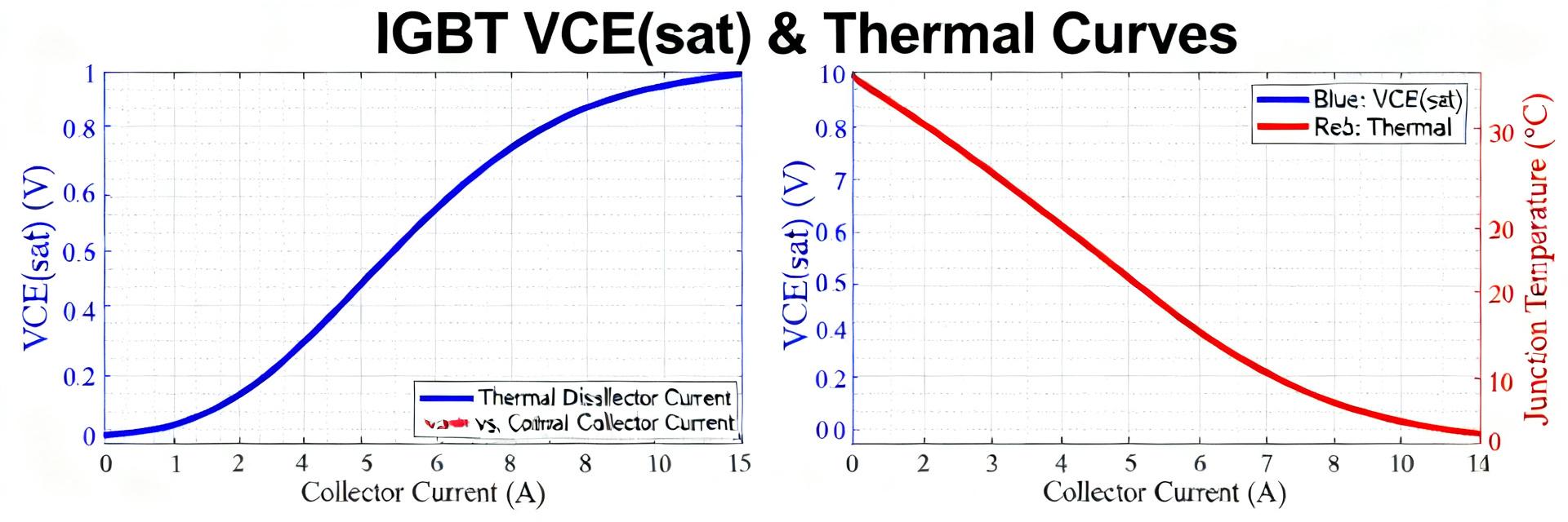
    引言: NGW75T65H3DFP 是一款 650 V 级、75 A 沟槽场截止 IGBT,额定结温高达 175 °C。准确的 VCE(sat) 表征和热建模决定了导通损耗、结温升以及长期可靠性;若对这两者估计错误,将导致过度发热、降额运行或现场故障。本文提供了关于 VCE(sat) 测量、Rth/Zth 解读以及实用三相逆变器示例的可测试指南。 引言:目标与方法 — 提供简明的规格快照、数据驱动的 VCE(sat) 趋势、稳态和瞬态热计算、实验室测量最佳实践,以及工程师可在实验室复现并应用于系统设计的实际热预算。 1 — 快速规格快照(背景) 关键电气额定值和运行范围 要点: 了解限制导通和开关的额定值。证据: 该器件列为 650 V 级、75 A 连续电流器件,具有高 TJ 限值。解释: 在设计人员使用数据手册中的 VCE(sat) 曲线预测损耗之前,必须检查 VCES/BV、IC(连续和脉冲)、VGE(max)、栅极阈值范围以及 SOA 说明。 参数 数值 / 备注 器件 NGW75T65H3DFP 集电极-发射极电压 (BV) 650 V 级 连续集电极电流 (IC) 75 A(受封装限制) 最大结温 (TJ max) 175 °C 热额定值与封装概述 要点: 热界面决定有效冷却效果。证据: 数据手册列出了 TJ max、推荐的 Tc/A 限值,通常还提供 Rth(j‑c) 和瞬态 Zth 曲线。解释: Rth(j‑c) 定义了到基板的热量路径;Rth(j‑a) 或壳到环境的热阻取决于安装方式和散热器;两者共同控制稳态 deltaT = P × Rth 并设定冷却要求。 2 — VCE(sat) 表征与趋势(数据分析) VCE(sat) 随 Ic 和结温的变化 要点: VCE(sat) 随 IC 升高而增加,也随更高的 Tj 而增加。证据: 数据手册中的 VCE(sat) 曲线显示,在高结温下导通电压具有正温度系数。解释: 在工作 Tj 下较高的 VCE(sat) 直接增加了导通损耗 Pcon = IC × VCE(sat),因此在稳态或循环负载下,热反馈可能加速发热。 解读测试条件并外推实际数值 要点: 数据手册中的“典型”和“最大”曲线使用指定的 VGE 和脉冲条件。证据: VCE(sat) 通常在 VGE = 15 V 下使用短脉冲测量,以避免自加热。解释: 通过考虑脉冲与直流加热的差异、制造离散度,并在预算导通损耗时使用裕量(例如,使用数据手册最大值 + 容差),将这些数值转换为稳态值。 3 — 热性能:稳态与瞬态(数据分析) 结到壳和结到环境指标 要点: 使用 Rth 指标将电气损耗转换为温升。证据: 数据手册提供 Rth(j‑c),有时也在定义的安装条件下提供 Rth(j‑a)。解释: 计算 Pconduction = IC × VCE(sat);然后 deltaTj‑c = P × Rth(j‑c)。加上壳温或散热器温度即可得到 TJ。这给出了指定冷却条件下的稳态限值。 瞬态热阻抗与功率循环 要点: 短脉冲需要 Zth(t) 而非稳态 Rth。证据: Zth(j‑c)(t) 曲线将能量映射为瞬态 deltaT。解释: 对于脉冲,计算 deltaT(t) = Ppulse × Zth(t)。对于孤立事件使用单脉冲 Zth,对于周期性占空比使用累积/多脉冲模型;热时间常数指导散热器质量和气流选择。 C (VCC) E (GND) G (IN) Kelvin E 4 — 测量方法:捕获 VCE(sat) 和热数据的实验室设置(方法/指南) 测试电路与仪器最佳实践 要点: 适当的硬件可防止测量误差。证据: 推荐设置包括受控电流源、栅极驱动器、开尔文传感和低电感布局。解释: 将器件安装在校准的冷板或散热器上,在推荐的参考点放置 Tc 传感器,使用短电流脉冲捕获无自加热的脉冲 VCE(sat),并测量环境和壳温以确保可追溯性。 数据记录、可重复性与有用曲线的推导 要点: 可重复的流程产生可靠的曲线。证据: 遵循分步流程:稳定器件,施加 VGE(例如 15 V),步进扫描 IC,记录 VCE 和 Tc,在不同基板温度下重复。解释: 汇编多个 Tj 点的 VCE(sat) vs IC 数据,拟合线性温度系数,并记录测量不确定性以用于设计裕量。 5 — 设计案例研究:三相逆变器导通与热预算(案例研究) 热计算实例 要点: 应用测得的 VCE(sat) 来计算结温升。证据: 选择代表性的每相 RMS 电流,并使用工作 Tj 下测得或数据手册中的 VCE(sat)。解释: 计算每个器件的 Pcon = IC_avg × VCE(sat);然后 TJ = Tc + P × Rth(j‑c)。在选择散热器或强制风冷参数时,为最坏情况的 VCE(sat) 和高环境温度添加裕量。 VCE(sat) 对系统效率和冷却选择的影响 要点: VCE(sat) 的小幅偏移会显著影响系统损耗。证据: 在 75 A 下,VCE(sat) 增加 0.1 V 会使每个器件增加 7.5 W 损耗;在整个逆变器桥臂中乘以这一数值是显著的。解释: 通过并联器件、改善热路径(降低 Rth 安装)、优化栅极驱动以最小化导通状态,或选择在预期 TJ 下测得较低 VCE(sat) 的部件来缓解。 6 — 实用清单:规格阅读、测试与热设计行动(行动建议) 工程师预选清单 要点: 简明的预检查可避免意外。证据: 确认 VCE(sat) 测试条件,核实 TJ max 和 Rth 值,并检查 SOA 和脉冲额定值。解释: 记录预期的工作 IC、最坏情况的环境温度、所需的降额,并搜索类似“NGW75T65H3DFP VCE(sat) measurement”的长尾查询,以便在团队笔记中捕捉细节。 PCB、安装与冷却最佳实践 要点: 机械和 PCB 决策决定 Rth(j‑a)。证据: 推荐做法包括大面积铜箔、多个过孔、正确的基板扭矩以及高质量的 TIM(导热界面材料)。解释: 按照数据手册放置 Tc 测量点,在运行中进行热剖面测试,并计划定期检查;如果循环严重,向供应商索取额外的瞬态 Zth 数据。 关键总结 在受控的 VGE 和 Tj 下进行准确的 VCE(sat) 测量,对于估算导通损耗并防止大功率转换器中的 NGW75T65H3DFP 发生热失控至关重要。 结合数据手册中的 Rth(j‑c) 和 Zth(t) 与测量的 P,计算稳态和瞬态 TJ;包含制造和测量裕量。 VCE(sat) 的小幅增加会放大冷却需求——尽早规划散热器、气流和布局,并通过实验室功率循环和热剖面进行验证。 常见问题解答 如何测量 NGW75T65H3DFP 的 VCE(sat) 以获得可靠数据? 使用开尔文传感技术和校准的 Tc 参考点,在数据手册规定的栅极电压(通常为 15 V)下,通过短且受控的电流脉冲测量 VCE(sat)。记录环境温度和壳温,步进扫描 IC,并在多个基板温度下重复测试,以推导温度系数并评估可重复性。 如何将数据手册中的 VCE(sat) 转换为稳态导通损耗? 在预期的 TJ 下使用保守的 VCE(sat) 值(数据手册最大值加上容差),乘以工作 IC 得到 Pcon。然后计算 deltaT = P × Rth(j‑c)(或 P × 到环境的总 Rth)以估算 TJ。为测量不确定性和可能的占空比加热增加裕量。 何时瞬态 Zth 对热分析至关重要? 当脉冲或变化的占空比主导加热时(短爆发、再生事件或功率循环),使用 Zth。对于单次事件,计算瞬态 deltaT = Ppulse × Zth(t);对于周期性脉冲,使用卷积或累积方法;仅在真正的直流条件下依赖稳态 Rth。 哪些设计步骤可以最小化高 VCE(sat) 对整体系统效率的影响? 通过并联器件、改善热路径(低 Rth 安装)、优化栅极驱动参数以最小化导通电压,以及在真实负载条件下通过精确的热剖面验证来缓解影响。 摘要 准确解读 NGW75T65H3DFP 的 VCE(sat) 数据,并正确使用 Rth 和 Zth 数值,对于预测结温并确保在全负载和高环境温度下的可靠运行至关重要。结合数据手册曲线与精确的实验室测量,应用保守裕量,并在设计冷却方案时使用已完成的计算和清单。
  • NGW75T65M3DFPQ 规格分析:关键电气参数

    Datasheet-reported metrics are the fastest way to judge whether a power transistor will meet a design’s voltage, current, switching, and thermal needs. This note uses NGW75T65M3DFPQ as the example device to show how to extract and apply specs and electrical metrics to real designs, prioritizing margin calculations and testable checks for US engineering teams. The goal is pragmatic: identify which datasheet sections map to design risks, calculate conduction and switching loss budgets, and define bench tests that validate manufacturer claims. The following sections walk a designer from reading tables and graphs to producing a loss/thermal snapshot and a test checklist. 1 — Background: What the NGW75T65M3DFPQ Specs Cover 1.1 — Key parameter categories to expect Datasheets group parameters into voltage ratings, current ratings, static conduction metrics (VCE(sat) or RDS(on)), dynamic switching metrics (Qg, Eon/Eoff), thermal resistances (RthJC, RthJA), and SOA/reliability data. Map each category to its datasheet section: electrical characteristics, dynamic characteristics, thermal data, and SOA. Treat each short definition as the basis for margin rules (blocking voltages, continuous current, transient handling). Annotated datasheet table — key specs (example) Parameter Typical / Example Notes Vceo / Vds 650 V Absolute blocking; derate to 50–80% of rating IC (continuous) 75 A Occurs at specified case temp; check RthJC VCE(sat) 1.2 V @ 25 A Used for conduction loss estimates Qg 60 nC Impacts gate-drive energy and switching loss RthJC 0.25 °C/W Key for junction temp calculations 1.2 — How to read datasheet tables and graphs Common graphs include transfer characteristics (IC vs. VCE at VGE), output curves (VCE vs. IC), gate-charge plots, and thermal impedance vs. frequency. Read axes, test conditions, and curve annotations: note ambient vs. case temperature, measurement points, and pulse widths. Annotate each graph with intended operating points so you can read off Eon/Eoff or slope values for dv/dt and di/dt analysis. 2 — Core Electrical Metrics Explained 2.1 — Voltage ratings and margins (VCEo, VGE(max), VCE(sat) implications) Voltage specs define blocking capability and gate limits; VCEo sets the maximum collector-emitter voltage, VGE(max) governs gate oxide limits, and VCE(sat) or RDS(on) controls conduction headroom. For margining, target 50–80% of VCEo as working voltage depending on transient exposure, and size snubbers or TVS to clamp expected spikes. Using electrical metrics this way prevents overstress during transients. 2.2 — Current, conduction losses and thermal limits (IC, continuous current, RthJC) Differentiate continuous IC from pulsed ratings; continuous current is limited by junction temperature via RthJC and cooling. Convert current into temperature rise with Pd × RthJC (or RthJA for board-mounted parts). Apply long-term derating—commonly 70–80% of continuous IC at rated case temperature—to improve reliability and avoid thermal runaway in high-power applications. 3 — Performance Analysis: Using Datasheet Graphs & Calculations 3.1 — Interpreting transfer/output curves and switching graphs Plot VCE vs. IC curves at your expected VGE and temperature to confirm conduction region behavior. For switching, read gate-charge curves to derive gate-drive energy (Egate = Vdrive × Qg) and use switching energy curves (Eon/Eoff vs. IC, VCE) to estimate per-switch losses. Always extract data at the pulse width and temperature closest to your operating case for accurate projections. 3.2 — Example calculations to prove suitability Use straightforward formulas: conduction loss Pcond = VCE(sat) × Iavg; switching loss Psw = (Eon + Eoff) × fsw. Estimate Tj: Tj = Ta + Pd × RthJA (or follow a chain Ta→Heatsink→Case→Junction for case-based). Below is a compact worked example using representative numbers to show the method. Loss and thermal calculation example (representative) Item Value Notes / Units Iavg 25 A Average device current VCE(sat) 1.2 V At test condition Pcond 30 W 1.2 V × 25 A Eon+Eoff 1.2 mJ Total per switching event fsw 50 kHz Switching frequency Psw 60 W 1.2e-3 J × 50e3 Hz Pd (total) 90 W Pcond + Psw RthJA 0.8 °C/W Board-mounted example ΔT 72 °C 90 W × 0.8 °C/W Tj ~142 °C Assumes Ta = 70 °F (~21 °C) plus ΔT GATE (G) COLLECTOR (C) EMITTER (E) IGBT 4 — Measurement & Test Methods 4.1 — Essential static tests to validate datasheet claims Bench tests should confirm VCE(sat)/RDS(on) at defined gate drive and at multiple temperatures. Use Kelvin sensing for low-resistance measurement, short pulse widths to avoid self-heating, and a calibrated thermocouple on the case. Scope probe grounding and snubber placement affect measured VCE(sat); document fixture parasitics and repeat tests at expected ambient and elevated temps. 4.2 — Dynamic switching tests and EMI considerations Capture switching transitions with proper probe bandwidth, use current probes for di/dt, and measure Eon/Eoff with known load inductance or clamp circuits. Evaluate dv/dt and di/dt against gate-drive thresholds to avoid false turn-on. Test with common snubbers and clamp configurations and monitor device case temperature during bursts to reveal thermal limits under realistic EMI and switching stress. 5 — Application & Selection Checklist 5.1 — Example application scenarios and selection rules Case 1: high-voltage inverter — prioritize VCEo margin, SOA for inductive turn-off, and switching energy at high VCE. Case 2: isolated SMPS — prioritize low conduction loss at average current, gate-charge for driver sizing, and RthJC for thermal path. For each use-case, check: voltage margin, peak/pulsed current, switching losses, SOA, thermal path, and gate-drive compatibility. Voltage margin — target 50–80% of VCEo depending on transient environment. Peak vs. continuous current — compare pulse ratings to expected surge conditions. Switching losses — compute Psw at intended fsw and include gate-drive energy. SOA and thermal path — verify junction temp and heatsink/case interface. 5.2 — Final design checklist & recommended deliverables Deliverables for selection: annotated datasheet excerpts keyed to your operating points, a loss budget table, measured test logs (static and dynamic), a thermal simulation snapshot, recommended derating percentages, and gate-drive/protection notes. These items allow peer review and create traceability for production qualification and reliability forecasting. Summary (conclusion) Use the NGW75T65M3DFPQ datasheet to extract blocking voltage, conduction metrics, switching energy, and thermal resistances and translate them into working margins and test points. Calculate conduction and switching losses, combine into a Pd and apply a thermal chain (RthJA or RthJC) to estimate Tj under expected cooling conditions. Validate with bench tests: Kelvin resistance checks, pulsed switching energy capture, and thermal monitoring; document results in a loss budget table for design sign-off. Frequently Asked Questions How do I verify NGW75T65M3DFPQ VCE(sat) measurement? Measure VCE(sat) with a pulsed test: apply the specified gate drive, use a short pulse to avoid heating, and sense VCE with Kelvin wiring at the device terminals. Record test pulse width, duty cycle, case temperature, and probe grounding. Repeat at elevated case temperature to capture temperature dependence and compare against datasheet conditions for accurate margining. What is a practical NGW75T65M3DFPQ thermal derating example? Derating example: if continuous IC rating is 75 A at 25 °C case, apply a 70% derating for long-life operation and higher ambient: plan for 52.5 A continuous. Combine with Pd calculation and RthJC to size heatsink so that Tj remains below your chosen limit (commonly 125–150 °C depending on reliability targets). Which electrical metrics matter most for selecting NGW75T65M3DFPQ in a high-voltage inverter? Prioritize VCEo margin, SOA under inductive turn-off, switching energy at the target VCE and IC, and thermal resistance (RthJC or RthJA) that defines junction rise. Also include gate-charge for driver power and check dv/dt immunity to avoid spurious turn-on. These metrics together determine survivability and efficiency in inverter environments. How do you calculate total power dissipation (Pd) for the NGW75T65M3DFPQ? Total power dissipation is determined using the formulas: conduction loss Pcond = VCE(sat) × Iavg and switching loss Psw = (Eon + Eoff) × fsw. Adding these two values yields total Pd (Pd = Pcond + Psw). Finally, use the thermal chain formula Tj = Ta + Pd × RthJA to estimate internal junction operating temperature.

  • RJH60D1DPP-A0 IGBT:性能与可靠性报告

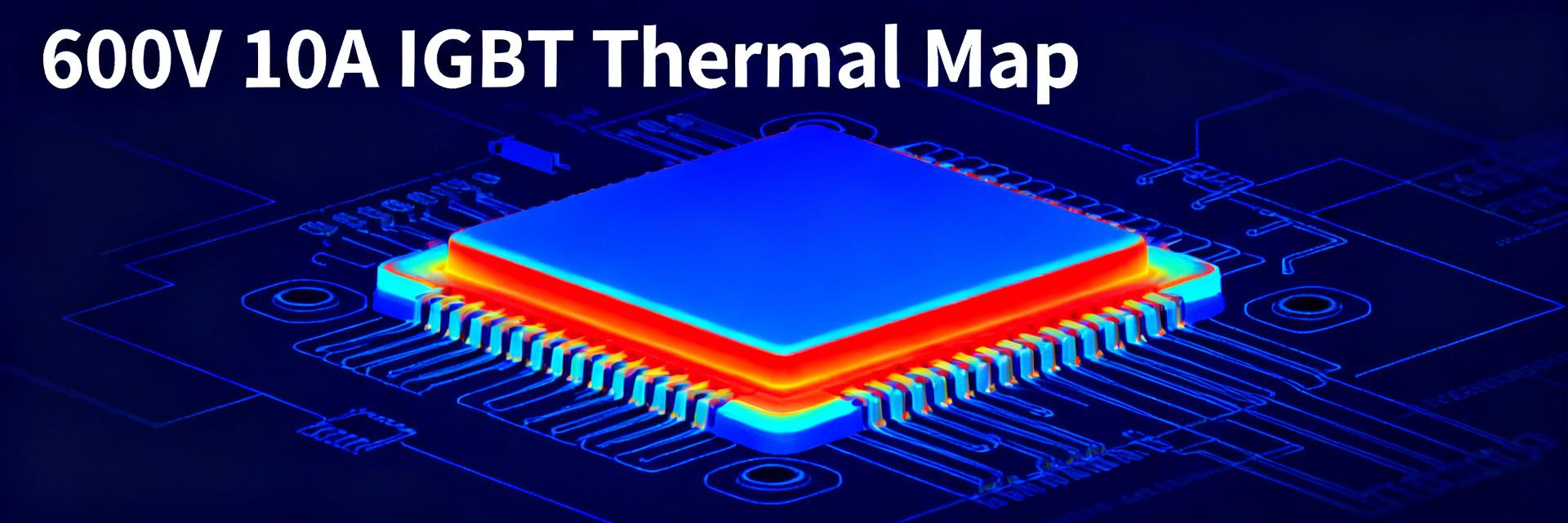
    器件亮点与预期:本报告首先介绍器件亮点,以构建系统级预期。制造商数据手册中列出了一款 600 V / 10 A 级器件,采用沟槽栅、薄晶圆结构,集成了快速恢复二极管,并具有低 VCE(sat)。这些已发布的属性为功率级电学基准测试以及热学/可靠性评估奠定了基础。 目的与范围:本报告为指定该 IGBT 的工程师提供测量和基准测试指南。独立的实验室式测试方案和数据手册图表被用作参考,以针对 RJH60D1DPP-A0 IGBT 在电学性能、热限制和可靠性驱动的设计选择方面提供可操作的建议,以便于量产集成。 背景与器件概述 技术摘要 关键电学和机械参数总结了器件定位。源自数据手册的数值(电压等级、额定电流、封装、推荐 Tj 范围、VGE(th)、集成二极管)提供了参考。这些规范将该器件置于典型的 600 V / 10 A 开关角色中,其中低 VCE(sat) 有利于导通效率,而沟槽栅薄晶圆几何结构平衡了通态损耗和开关速度。 参数 标称值 电压等级 600 V(数据手册) 集电极电流 10 A 连续(数据手册) 封装 模塑功率封装(数据手册) 推荐 Tj -40 至 +150 °C(数据手册) 显著特点 沟槽栅、薄晶圆、集成快速恢复二极管 目标应用与系统角色 典型应用范围决定了测试条件。制造商将该器件定位于电机驱动、逆变器、SMPS 和工业开关。使用场景范围——600 V 阻断、高达 20–30 A 的短期脉冲电流、高达数十 kHz 的 PWM 开关——为工作台搭建提供了信息,并有助于确定设计人员何时应选择此器件,而非速度更快但 VCE(sat) 更高的替代方案。 G C E 性能基准与电学表征 静态特性与直流性能 静态指标决定了导通和漏电预算。数据手册中的 VCE(sat) 对 IC 以及 VGE(th) 曲线作为可重复的参考,而工作台的可重复性依赖于开尔文(Kelvin)测试。在指定的栅极驱动(例如,VGE = 15 V)和 Tj 条件下测量 VCE(sat)、监测与 IC 相关的漏电流,并记录安全工作区(SOA)合规性,有助于规划保守的连续和脉冲工作点。 动态开关与二极管行为 开关能量和二极管恢复确立了损耗与 EMI 的权衡。数据手册中的开关波形以及独立工作台的 Eon/Eoff 和反向恢复曲线引导了预期。通过运行感性关断以在指定的负载、L 和栅极电阻下捕获 Eon/Eoff 以及二极管 trr,这一实用的 IGBT 性能评估确定了驱动器调节和缓冲电路的需求。 热性能与可靠性指标 热行为与降额 热阻和瞬态阻抗驱动着散热设计。数据手册中的结到外壳热阻和近似的 Zth 曲线是基准,通过热点的红外(IR)成像进行验证。在实际安装条件下,根据功率损耗和 Rth(j-a) 计算稳态 Tj,执行功率阶跃瞬态热阻测量,并应用保守的降额(例如,在高环境温度下降低连续电流),可确保实现最佳的 600V 10A IGBT 热管理。 可靠性测试与预期失效模式 加速测试揭示了主要的磨损机制。根据可靠性实践和数据手册中的鲁棒性说明,推荐进行标准的 HTOL(高温运行寿命)、温度/功率循环以及雪崩裕度测试。定义验收标准(例如 VCE(sat) 漂移限制和漏电流阈值)、规划样本量和测试持续时间,并将 RJH60D1DPP-A0 的可靠性测试重点放在键合线剥离、栅极氧化层退化和热失控前兆上,可确保长期部署的稳定性。 应用级评估:系统内测试案例 电机驱动使用案例 逆变器工作台方案模拟了实际的工作制。电机驱动中典型的三相 PWM、开关频率和峰值电流为测试选择提供了信息。使用代表性的 PWM 方案配置测试,在集电极/发射极/栅极/散热片上布置仪器,并对热负载曲线进行循环,可以验证动态驱动条件下的效率、热裕度和 EMI。 SMPS / 逆变器工作台案例 硬开关 SMPS 测试会对开关和恢复产生应力。来自工作台的效率与负载曲线以及瞬态过冲指标验证了缓冲电路和栅极驱动器的选择。使用明确的负载阶跃、测量瞬态恢复以及调节栅极电阻和缓冲电路拓扑,可在平衡开关损耗和 EMI 的同时,最大限度地减少过冲和振铃,从而实现目标变换器效率。 对比案例研究与现场失效模式 同类器件对比性能 同等条件下的比较需要完全相同的测试条件。在器件间的工作台评估中,采用相同的封装安装方式、测试波形和热环境。通过标准化模板比较 VCE(sat)、Eon/Eoff 以及瞬态热阻,可以进行快速的横向评分,以决定导通损耗与开关速度之间的权衡。 指标(测试条件:Tj = 25°C, VGE = 15V) RJH60D1DPP-A0 竞争对手替代方案 VCE(sat) @ IC = 10A 1.6 V(典型值) 1.9 V(典型值) Eoff @ 10A 感性负载 0.12 mJ(工作台实测) 0.09 mJ(工作台实测) 热阻 (Rth(j-c)) 3.2 °C/W 2.8 °C/W 观察到的现场失效模式与缓解措施 现场问题主要集中在热学和驱动缺陷上。常见报告提到过温、降额不足、雪崩过应力以及栅极驱动异常。溯源热界面、布局回路电感和电流检测可提供根本原因解决方案。直接的缓解措施包括改进 TIM(热界面材料)、收紧降额裕度以及调整栅极电阻,以减轻应力并提高 MTTF(平均无故障时间)。 实用建议:设计、测试与采购清单 可靠集成设计清单 特定的设计规则可减少早期失效。工作台关联表明,栅极驱动器配置和回路电感主导了开关过冲和应力。推荐的步骤包括选择平衡 dv/dt 和开关损耗的栅极电阻范围、利用合适的缓冲拓扑、最小化回路电感、遵循散热器安装扭矩/TIM 规范,并在 BOM 级设计中应用保守的电流/温度降额规则。 质量保证(QA)与来料检验/测试清单 来料验证可防止批次级异常。针对数据手册限制的功耗和热学/短路检查可发现质量偏差。定义抽样率,运行 VCE(sat)、漏电流和短路测试,要求供应商提供数据手册参数和批次可追溯性,并在监测长期 IGBT 性能趋势的同时记录偏差以作为采购决策依据。 总结 本技术报告综合了数据手册基准和工作台测试方法,以评估核心风险:热限制、栅极驱动调节以及二极管恢复效应。工程师应在最终 BOM 签发前执行两个系统内测试(电机逆变器和 SMPS)以及瞬态热阻测量;在进行适当降额和散热的情况下,RJH60D1DPP-A0 IGBT 可可靠地适用于 600 V / 10 A 的应用角色。 在选择驱动器之前,通过受控的开尔文感应测试方案对导通和开关损耗进行基准测试,以确认数据手册中的 VCE(sat) 和开关能量;这验证了 IGBT 在目标负载曲线下的性能。 进行瞬态热阻映射和保守的结温降额,以防止键合线剥离和热失控;记录 TIM 和安装扭矩以保证量产的可重复性。 执行加速可靠性测试(功率循环、HTOL、雪崩裕度),制定明确的验收标准和抽样方案,以验证批次质量和预期现场寿命。 常见问题解答 哪些测试条件最能揭示 RJH60D1DPP-A0 的热限制? 在固定环境温度下使用稳态功耗并测量 Rth(j-a),再加上通过红外成像捕获的功率阶跃瞬态过程。这结合了稳态降额和瞬态热阻,以设定连续电流限制和冷却要求。 如何选择栅极驱动设置以获得最佳 IGBT 性能? 从适中的栅极电阻开始,以平衡开关损耗和过冲,然后在感性负载下扫频 Rg 并记录 Eon/Eoff 和电压过冲。在不导致开关损耗不可接受地增加的情况下,针对最小 EMI 进行优化。 哪些验收标准可以检测来料检验中的早期批次问题? 指定 VCE(sat) 容差、正向漏电限制以及短路承受时间阈值,并与数据手册中的数值进行对比。拒收或隔离超出定义漂移的批次,以避免现场失效并保持可追溯性。 集成快速恢复二极管在 RJH60D1DPP-A0 中起什么作用? 集成快速恢复二极管作为反向并联续流路径,平衡了反向恢复电荷 (Qrr) 和软恢复性能。这限制了硬开关感性间隔期间的电压尖峰、瞬态开关噪声和 EMI。
  • MPMT1002QT0 表面贴装技术(SMT)完整规格与性能报告

    The MPMT1002QT0 delivers precision in compact SMT packages: typical TCR ~5 ppm/°C, power per element 125 mW (deratable), and operating temperature range −55°C to +155°C, making it relevant for high-accuracy sensor front-ends. This article analyzes full electrical and thermal specs, production test methods, and placement guidance to help PCB designers, process engineers, and procurement teams evaluate SMT performance and assembly risk for the MPMT1002QT0. Readers will find actionable test procedures, derating guidance, and a production checklist tailored to thin film resistor networks used in precision voltage dividers and measurement circuits. The report emphasizes SMT performance metrics designers should request from vendors and the PCB-level checks that minimize drift and field failures. 1 — Why MPMT1002QT0 Matters for SMT Assemblies 1.1 Component class & primary applications Point: MPMT1002QT0 is a multi-element thin film resistor network optimized for precision SMT use. Evidence: thin film resistor construction yields low TCR and tight stability versus thick-film alternatives. Explanation: designers use these networks in voltage dividers, sensor front-ends, and matched resistor arrays where ratio stability and low noise matter. Footprint: compact network package suitable for 0805-equivalent arrays Pin count: multi-terminal array (common configurations 4–8 terminals) Body size: small body height to fit low-profile assemblies 1.2 Key electrical & environmental specs at a glance Point: Quick spec snapshot helps part selection. Evidence: core specs designers request include resistance values, tolerance, TCR (ppm/°C), power per element, and operating temperature range. Explanation: the table below provides a compact reference for PCB layout and thermal planning. Spec Typical / Range Resistance values 10 Ω – 200 kΩ (array-dependent) Tolerance ±0.1% to ±1% TCR ~5 ppm/°C (typical) Power per element 125 mW (deratable with board temp) Operating temp −55°C to +155°C 2 — Full Electrical Specs & What They Mean for SMT Performance 2.1 Resistance, tolerance, TCR and their PCB-level impact Point: Resistance range and tolerance directly set circuit accuracy; tight tolerances reduce calibration effort. Evidence: a ±0.1% divider resistor yields
  • SOMC160310K0GRZ 完整数据手册:电气规格

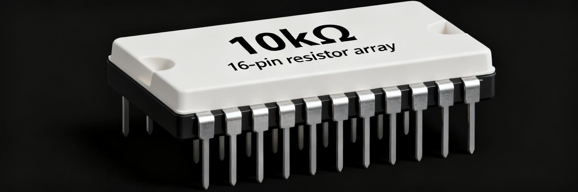
    According to the SOMC160310K0GRZ datasheet, this eight‑resistor network is specified as 10 kΩ ±2%, 160 mW power per element, and 100 ppm/°C TCR in a 16‑pin dual‑in‑line package—electrical specs that make it suitable for compact divider arrays and multi‑channel pull‑ups. This introduction summarizes the most relevant electrical numbers and why they matter for board designers and system accuracy. Key electrical specs and practical limits drive layout, thermal margin and test methods. This guide breaks down the numbers from the current datasheet, reconciles voltage vs. power limits, and gives concrete selection, layout and test guidance engineers can apply directly during validation and production. 1 — Product overview & quick electrical summary (background) 1.1 Quick-specs table (must-have numbers) Parameter Typical / Nominal Absolute / Max Units / Notes Resistance (per element) 10 kΩ — Ω (datasheet) Tolerance ±2% — (datasheet) Power rating (per element) 160 mW — mW (datasheet) TCR 100 ppm/°C — ppm per °C (datasheet) Max voltage (absolute) — 50 V (datasheet) Package / pins 16‑pin dual‑in‑line — DIP / SIP family (datasheet) Operating temp −55 to +155 — °C range (datasheet) Isolation between elements Specified per datasheet — Resistance to adjacent elements (datasheet) 1.2 Package & pinout overview The network is supplied in a 16‑lead dual‑in‑line package with standard 0.1‑inch lead spacing; pin assignments place resistor ends on adjacent pins across the package body. Mechanical tolerances and pin‑to‑pin isolation values are listed in the datasheet; designers should reference the recommended PCB footprint and maintain consistent solder fillets and thermal reliefs to avoid mechanical stress or thermal coupling between elements. R1 1 (IN1) 16 (OUT1) 8 (IN8) 9 (OUT8) 2 — SOMC160310K0GRZ datasheet — Detailed electrical specifications (data analysis) 2.1 Resistor element characteristics Resistance tolerance ±2% sets nominal matching; TCR of 100 ppm/°C means a 10 kΩ element shifts ~1 Ω per 1°C change. Power limits and voltage constraints interact: use P = V² / R and Vmax_power_limited = sqrt(P_rating × R). For 10 kΩ at 160 mW: Vmax_power_limited ≈ sqrt(0.16 × 10000) = 40 V, below the datasheet absolute‑max voltage of 50 V. The difference reflects separate constraints—steady‑state power dissipation vs. dielectric/flashover limits—so both must be respected in designs. 2.2 Operating/environmental and reliability specs The current datasheet lists wide operating temperatures (down to −55 °C and up to +155 °C) and soldering/reflow profiles for reliability. Thermal resistance and derating information are provided; read derating curves to shift allowable continuous power at elevated ambient temperatures. Storage and mechanical shock specs guide handling: follow recommended solder profiles to avoid resistance shifts from thermal stress. 3 — Performance characterization & test guidance (data analysis / method) 3.1 Typical performance graphs & what to expect Datasheet graphs typically show resistance vs. temperature, long‑term stability and short‑term drift. Expect tens to hundreds of ppm drift over thousands of hours depending on mounting and ambient. For ADC or sensor references, translate ppm drift into LSB error at the system ADC range; use the resistance vs. temperature curve to predict worst‑case offset across the operating range and add margin accordingly. 3.2 How the datasheet tests specs (measurement methods) Typical test methods include four‑wire (Kelvin) resistance measurement, defined test voltages/currents, and thermal soak to stabilize readings. For validation, measure each element with a calibrated DMM or LCR meter, perform thermal step tests, and record drift after reflow. A practical test checklist: 4‑wire DC resistance, power dissipation test at expected current, thermal cycling and post‑reflow resistance comparison against datasheet limits. 4 — Application guidelines & circuit examples (methods / case) 4.1 Typical application circuits and layout tips Common uses: multi‑channel pull‑ups, resistor ladder for ADC reference, and input termination arrays. Example schematic snippet for a 4‑channel pull‑up: each element from IO pin to VCC. Layout tips: group network close to the IO header, match trace lengths for ladder accuracy, and provide thermal relief to prevent power dissipated in one element from heating adjacent elements and skewing values. 4.2 Thermal management, derating calculations & safety margin examples Derating example: with 160 mW rating and board conditions that reduce dissipation capability, target 50% margin for continuous loads → allowable per element ≈80 mW. If element dissipates P_expected = V²/R, solve for V: V_allowed = sqrt(P_allowed × R). For 10 kΩ and 80 mW, V_allowed ≈ sqrt(0.08×10000)=28.3 V. Always check both power‑limited and absolute voltage limits. 5 — Selection checklist, troubleshooting & procurement notes (action) 5.1 Quick selection checklist Confirm required resistance & tolerance match the network nominal value and tolerance. Verify power per element plus margin (recommend ≥50% for continuous use) against expected dissipation. Check TCR requirement for temperature sensitivity and system accuracy needs. Confirm package/pinout fits board footprint; review datasheet mechanical drawing before layout. Red flags: dissipation near rating, high ambient temp, or pinout mismatch. 5.2 Common issues and fixes (troubleshooting) Typical problems include post‑reflow resistance shift (solder stress), thermal coupling causing element-to-element drift, and measurement errors from two‑wire methods. Fixes: use four‑wire measurements, add thermal barriers or spacing between dissipating elements, follow recommended reflow profile, and replace suspect parts showing out‑of‑spec drift. When isolating faults, test the component off‑board to separate board vs. part issues. Summary (conclusion & call to action) The SOMC160310K0GRZ electrical specs—10 kΩ ±2%, 160 mW/element and 100 ppm/°C TCR—define suitability for compact divider arrays and pull‑up banks and set thermal and accuracy constraints. Power vs. voltage limits must both be checked: use P = V²/R and Vmax_power_limited = sqrt(P_rating × R) and then reconcile with the absolute voltage in the datasheet. Layout and thermal management (spacing, thermal reliefs, derating margins) directly impact long‑term stability and measurement accuracy in ADC or sensor front‑ends. Engineers should consult the current datasheet for final confirmation of pack, mechanical and electrical figures before finalizing layouts or procurement; verify power margins and perform four‑wire validation on assembled boards to ensure conformance. 6 — Common questions What are the typical power and voltage limits for SOMC160310K0GRZ? Per the datasheet the per‑element continuous power rating is 160 mW and the absolute voltage limit is listed as 50 V. For steady‑state operation use the power‑limited voltage calculation V = sqrt(P_rating×R) to avoid exceeding dissipation even when absolute‑voltage appears permissible. How does TCR affect precision applications using this resistor network? A TCR of 100 ppm/°C implies noticeable drift over large temperature swings: for 10 kΩ, a 50 °C change yields ~5000 ppm (0.5%) shift if unmitigated. For precision ADC references, compensate by design (temperature compensation, calibration, or selecting tighter TCR) or by limiting operating temperature swings. What test steps should be included to validate SOMC160310K0GRZ on a populated board? Validation steps: four‑wire resistance baseline, post‑reflow comparison, thermal soak and step tests, and powered stress at expected application voltage with monitoring. Record deviations vs. the datasheet claims and ensure margins for continuous dissipation and ambient temperature are maintained. How do you layout the SOMC160310K0GRZ to prevent thermal coupling? To prevent thermal coupling and drift, group the network close to the IO header, match trace lengths for ladder accuracy, and provide physical spacing or thermal barriers between dissipating elements. Standard thermal reliefs should be used on all pin footprints.