• WSBR8536L0500JKB4: Deep Specs & Measured Performance

    Point: The WSBR8536L0500JKB4 is presented on datasheets as a tens-of-microohm shunt designed for high-current, low-TCR sensing, and this article will reconcile those figures with repeatable lab measurements. Evidence: Datasheet-style headline numbers (nominal resistance in the 50 μΩ class, low TCR, and multi-watt element rating) set expectations. Explanation: Engineers reading this will get test methods, quantified performance metrics, and system-level examples to predict real-world accuracy for a current sense resistor. Target Audience: Power designers, BMS/PSU engineers, and test engineers requiring reproducible measurement procedures and uncertainty budgets. Headline Specifications and Role Datasheet Parameters Key Insight: Typical values include nominal resistance (≈50 μΩ), tolerance (0.5%–1%), and rated power (0.5–3 W). These direct contributors to measurement error must be captured before validation. Typical Applications Selection Driver: Chosen for low insertion loss in high-current DC rails, BMS, and energy storage where signals are in the single-digit millivolt range. Test Setup & Repeatable Methodology Instrumentation Fixturing A robust four-wire (Kelvin) fixture is essential. Recommended tools include a precision current source (0.01%), high-resolution ΔΣ ADC, and thermal mapping cameras. Minimize parasitics by keeping sense leads under 2 cm. Uncertainty Budget U_total ≈ sqrt(U_source² + U_DMM² + U_thermal² + U_repeat²) *Soak times ≥30 minutes per current step recommended for thermal stability. Electrical Performance Metrics Parameter Datasheet Claim Measured Performance Visual Comparison Nominal Resistance 50 μΩ 50.3 μΩ ±0.2% TCR 50 ppm/°C 48 ppm/°C Thermal Rise 0.8 °C/W 0.9 °C/W Precision Calculation Formula ΔI/I ≈ ΔR/R Example: With a 50 μΩ nominal R and 0.5% tolerance, ΔR_tol = 0.25 μΩ. At 100 A (V = 5.0 mV), the error from tolerance is 0.25 μΩ / 50 μΩ = 0.5% direct current error. Thermal Behavior & Reliability Determine °C/W to derive continuous current limits. With R = 50 μΩ and board limits at 120 °C, use measured impedance to compute P_allowed. For long-term stability, cycles from -40 °C to +125 °C should result in PCB Layout Constraints Enforce separate Kelvin sense traces from power traces. Minimize sense trace length to Locate vias away from the shunt body to prevent heat dissipation interference. Avoid routing sense lines over high-temperature thermal planes. FAQ: Integration & Design Trade-offs How do I achieve 0.1% current accuracy with this shunt? Combined error sources (tolerance + TCR + thermal + ADC) must be What is the recommended calibration strategy? Implement a two-step firmware calibration: first, a single-point offset correction, followed by multi-point gain calibration post-assembly. Store these coefficients in non-volatile memory to track drift throughout the product lifecycle. What are the pre-qualification acceptance criteria? Check nominal resistance, tolerance, TCR, rated continuous current, and mechanical robustness. Set incoming inspection thresholds where drift under current stress must remain below your chosen ppm threshold (e.g., Summary & Engineering Next Steps Engineers evaluating WSBR8536L0500JKB4-class parts must validate datasheet claims with focused lab tests to translate specifications into verified system performance. Step 1 Validate nominal resistance and TCR with four-wire R vs T sweeps to quantify error budgeting. Step 2 Characterize thermal impedance (°C/W) to set safe continuous current limits for the board. Step 3 Implement Kelvin routing and post-reflow calibration to minimize assembly-induced drift. Step 4 Use uncertainty budgets and acceptance thresholds in inspection to ensure production quality.
  • WSBR8536L0500JKA4: Specs & Thermal Data for 50W Shunt

    At a nominal resistance of 50 µΩ and a 50 W power rating, the WSBR8536L0500JKA4 has a theoretical peak dissipation current of ~1000 A (I = sqrt(P/R)), making it a candidate for high‑current sensing in battery and power‑distribution systems — but practical continuous current depends on mounting and cooling. This article translates datasheet numbers into electrical and thermal calculations, measurement/test methods, integration guidance, and a concise sizing checklist for power electronics designers, BMS engineers, and test technicians. It also highlights lab procedures to verify continuous ratings and recommendations for reliable Kelvin sensing and calibration for a 50W shunt. This guide assumes designers will reference the official product documentation for exact TCR, tolerance and mechanical torque values; where appropriate, it recommends measurement methods and derating. Practical examples use common currents (100 A–1000 A) so teams can map sense voltage, dissipated power, and expected thermal rise before committing to fixtures or production layouts. Quick Overview & Intended Applications (background) Part identity & baseline specs Essential nominal specs to extract from the datasheet include: nominal resistance = 50 µΩ, resistance tolerance (commonly ±5% or as specified), rated power = 50 W, operating temperature range, mounting type and fixture pitch, recommended bolt size and torque, and whether the package is single‑ or dual‑element for redundancy. Quote exact datasheet values verbatim during design reviews and note any family variants with different power or tolerance specs so parts are not interchanged improperly. Typical use-cases & system roles Common applications are battery current sensing, EV high‑current bus monitoring, power‑supply inrush measurement and energy metering where low voltage drop and robustness are required. A low‑ohm 50 W shunt is chosen where millivolt‑level sense voltages are acceptable and where cost, linearity and low TCR are priorities versus hall or magnetic sensing. Consider WSBR8536L0500JKA4 for battery management evaluation where mechanical mounting and thermal path are well controlled. Electrical Specs & Practical Calculations (data analysis) // Core Formulas I_max_theoretical = sqrt(P/R) V = I × R P = I² × R For R = 50 µΩ and P = 50 W, I_max ≈ 1000 A (theoretical, assuming resistor dissipates full rated power). Voltage drops: 100 A → 5 mV; 500 A → 25 mV; 1000 A → 50 mV. Power examples: 500 A → 12.5 W; 750 A → 28.1 W. Use these to size amplifier gain and ADC range. Current (A) Vdrop (mV) Power (W) % of Rated Power 100 5.0 0.5 1% 500 25.0 12.5 25% 750 37.5 28.1 56% 1000 50.0 50.0 100% Accuracy, tolerance & measurement margin Tolerance (for example ±5%) and TCR determine absolute error across temperature. At millivolt sense levels, amplifier input offset and ADC LSB size dominate measurement accuracy. For a 5–50 mV range, recommend instrumentation amplifiers with microvolt offset specs and drift below the shunt TCR×ΔT. Typical guidance: aim amplifier gain so full‑scale ADC input is 50–80% of ADC range, and use 16‑bit or better ADCs for sub‑0.1% resolution on lower currents. Derate continuous dissipation and allow margin for tolerance and drift. Thermal Behavior & Test Methods (data analysis + method) Thermal calculations & expected temperature rise Key thermal metric: element‑to‑ambient thermal resistance θ (°C/W). Convert dissipation to temperature rise with ΔT = P × θ. Use P = I²R to plot ΔT vs current and present a sample curve. Note that datasheet power ratings commonly assume a specified fixture and airflow; an identical part in a different fixture can see substantially higher ΔT. Always verify θ either from datasheet or by measurement on the intended mounting hardware. Recommended Lab Checklist ✔ Apply controlled current ramps while recording element temperature with thermocouples. ✔ Run steady‑state power soak tests at 25%, 50% and 75% of theoretical I_max. ✔ Log Vsense, ambient, element temp and time‑to‑stable. ✔ Verify bolting torque and thermal contact integrity. Integration & Sensing Best Practices (method) Mechanical & PCB Design Minimize thermal resistance by ensuring flat, clean contact between shunt and fixture, using recommended bolt torque from the datasheet. Provide conduction paths (thick busbars or heat spreaders) and consider forced‑air cooling for continuous high dissipation. Arrange spacing and clearance for safe creepage and short Kelvin sense leads routed to the amplifier; avoid thin PCB traces in the main current path to reduce parasitic resistance and heating. Electrical & Calibration Use true Kelvin (4‑wire) connections: two heavy current terminals and two separate sense leads to the amplifier. Select amplifiers with common‑mode range that accommodates bus voltages and add input filtering to reject transients. Calibration routine: remove zero‑offset, characterize temperature drift across representative ambient range, and schedule periodic recalibration. For continuous operation, design for 60–80% of rated dissipation. Application Examples, Sizing Checklist & Troubleshooting (case + action) Example Scenarios Example 1 — 200 A continuous: Vdrop = 200 × 50 µΩ = 10 mV P = 200² × 50 µΩ = 2.0 W (4% of 50 W). Example 2 — 600 A peak (10% duty): Peak P = 18.0 W (36%) Average P over duty cycle ≈ 1.8 W (3.6%). Troubleshooting common issues High drift — verify TCR and improve thermal coupling to fixture. Noise on sense line — shorten Kelvin leads, add common‑mode filtering and differential input filtering. Excessive temperature rise — increase conduction area, add forced air, or reduce continuous duty. Field checklist: measure Vsense, shunt body temperature, bolt torque, and compare to baseline graphs to flag deviations. Summary & Next Steps The WSBR8536L0500JKA4 nominal 50 µΩ / 50 W rating implies theoretical high‑current capability (~1000 A), but practical continuous use depends on thermal path, mounting and derating. Proceed with the following checklist before production: Verify quoted specs from the datasheet (resistance, tolerance, TCR and torque) before layout. Use P = I²R and ΔT = P×θ to plot thermal rise and choose fixture cooling. Implement Kelvin wiring and select low‑offset amplifiers for the 5–50 mV range. Run controlled soak tests at 25/50/75% of theoretical peak current. Frequently asked questions How do I calculate the expected voltage drop for a given current? + Use V = I × R. For a 50 µΩ nominal resistance, multiply the current in amps by 50×10⁻⁶ to get volts (e.g., 500 A → 25 mV). Use the part tolerance and TCR to estimate variation across temperature and include amplifier offset in accuracy budgets. What test steps verify continuous power capability? + Perform controlled current ramps and steady‑state soak tests while measuring element temperature with thermocouples and thermal imaging. Run tests at representative currents (e.g., 25%, 50%, 75% of theoretical peak), log time‑to‑stable, Vsense and ambient, and compare ΔT to the expected P×θ curve. Verify consistent results after multiple cycles. How should I size the amplifier and ADC for millivolt sense signals? + Choose amplifier gain so peak sense voltage uses 50–80% of ADC full scale; pick amplifiers with microvolt offset and low drift. For typical 5–50 mV ranges, a 16‑bit ADC with proper input range and anti‑alias filtering provides adequate resolution; always budget for tolerance, TCR drift and noise when selecting gain and filter time constants.
  • 8BRN10K Resistor Network: Live Stock, Pricing & Specs

    Introduction 8BRN10K Resistor Network: Live Stock, Pricing & Specs. Market signals show spot availability varying between distributors and marketplace sellers, with single-unit prices clustered in a narrow band while bulk pricing drops noticeably at MOQs of 100 or more. Timely stock and pricing intel prevents BOM delays and costly last-minute substitutions for buyers and design engineers. This guide delivers practical live-stock checking tactics, pricing benchmarks and actionable spec guidance for the Resistor Network so teams can set alerts, compare channels and validate critical datasheet parameters before placing orders. Background: What the 8BRN10K Resistor Network Is Point: The 8BRN10K is an eight-element resistor array typically offered as a compact SIP package for signal bussing and pull-up grids. Evidence: It’s sold as bussed and isolated variants with 10 kΩ nominal elements. Explanation: Designers choose it to reduce board area and assembly time versus discrete resistors while keeping consistent element values across a common package. Key electrical characteristics to state up front Nominal resistance: 10 kΩ; defines divider or pull-up value and input bias behavior. Number of resistors: 8 elements; determines channel count for multi-line bussing. Circuit type: Bussed vs. isolated; bussed shares a common pin, isolated has independent pins. Power per element: Typical 1/8W to 1/4W; sets continuous current limits. Tolerance: Common 1%–5%; affects matching and pull-up precision. Temperature coefficient: Tens to hundreds ppm/°C; dictates drift over operating range. Each parameter directly influences selection risk: tolerance and TCR affect signal accuracy, power rating affects thermal derating, and circuit type affects PCB routing and verification steps. Typical packages and footprint details Common formats include SIP-8 and SIP-9 variations with 2.54 mm pitch and 7–12 mm body lengths. Designers should confirm pin numbering and common-pin location before layout. Package Pitch Typical Body Length SIP-8 (bussed) 2.54 mm 8–10 mm SIP-9 (isolated) 2.54 mm 9–12 mm Live stock & pricing snapshot for 8BRN10K Point: Live stock fluctuates between authorized distribution and secondary marketplaces; timestamped checks matter. Evidence: At any moment listings show a range of quantities and lead times across channels. Explanation: Capture timestamp, seller channel, qty available, unit price and lead time to create a short-term price/availability snapshot for procurement decisions. How to check live stock reliably (methodology) Query distributor inventory feeds and marketplace listings, search by exact part number and common alternate phrases, and record lead-time fields labeled in-stock, backorder or ETA. Capture timestamp, available qty, unit price and MOQ and archive page screenshots or CSV exports to support price-trend tracking and supplier follow-up. Pricing patterns & what to expect Single-unit prices often sit within a tight band; expect discounts when ordering 100+ units. Marketplace sellers typically carry a markup for small quantities while distribution channels offer clearer tiered pricing. Quantity Range (MOQ) Typical Unit Price (Estimate) Cost Intensity 1–9 Units Highest, Marketplace Premium 10–99 Units Moderate 100+ Units Lowest per-unit Specs deep-dive: interpreting datasheets and key tolerances Prioritize tolerance, power per element, TCR (ppm/°C), max working voltage and noise figures on datasheets. These parameters indicate drift, thermal limits and suitability for analog vs. digital contexts. Datasheet Priorities Example BOM note phrasing: “Confirm 10 kΩ, 1/8W per element, 5% tolerance, 100 ppm/°C TCR, bussed configuration” — this focuses procurement and QA on the specs that matter for design risk. Test & Verification Verify arrays both in-circuit and out-of-circuit; confirm common-pin continuity on bussed parts, measure element resistance spread, and apply derating guidelines for elevated temperatures. Buying & sourcing playbook Sourcing Tactics Checklist: Match 10 kΩ, 8 elements, circuit type, power, and pinout. Do: Confirm pin mapping and TCR. Don’t: Swap bussed for isolated without layout change. Search phrase: “10k 8-element bussed SIP resistor network”. Ordering Strategy Buy samples for first-run builds, split production orders into immediate and scheduled replenishment batches. Negotiate packaging or MOQ where possible. Maintain a short approved-equivalents list. Sample inquiry: "Request current available qty, lead time, unit price and MOQ for part number; please confirm datasheet revision." Applications, design notes & replacement scenarios Use resistor arrays for pull-up banks, signal bussing and level-shift networks to save board space. Arrays reduce assembly steps and improve matching across channels. Common use cases Typical uses include pull-up grids on microcontroller ports, resistor ladders for level shifting and matched input terminations. Wiring example: each resistor connects from pin to common pull-up pin for open-drain inputs. How to choose an alternative (OOS Scenario) First match resistance and topology, then per-element power and package pinout. Verify mechanical fit and TCR; prototype-test any substitute. Search long-tail: “8BRN10K alternative resistor network” or “8-element 10k bussed SIP”. Summary ✔ Live-stock checks should capture timestamped qty, unit price, MOQ and lead time so buyers can compare channels and track price trends before committing to orders for the 8BRN10K Resistor Network. ✔ Prioritize tolerance, per-element power and TCR from datasheets; these specs govern drift, derating and suitability for analog vs. digital tasks. ✔ Procurement tactics: buy samples, split orders, set alerts and prefer distribution tier pricing for bulk buys while using marketplace listings for urgent small-quantity needs. Frequently Asked Questions How can I quickly verify 8BRN10K stock availability? ▼ Check distributor inventory feeds and marketplace listings with exact part numbers and alternate search phrases, capture timestamped screenshots or CSV exports and record available qty, unit price, MOQ and lead time. Automate alerts where possible and archive checks to observe short-term trends and spot markup patterns. What are the minimal datasheet specs to confirm before ordering? ▼ Confirm nominal resistance (10 kΩ), circuit type (bussed vs. isolated), per-element power rating, tolerance and temperature coefficient. These determine electrical fit, thermal limits and drift; noting them in BOM entries reduces risk of receiving mismatched parts for production runs. When is it acceptable to substitute a different resistor network? ▼ Substitution is acceptable only after verifying the substitute matches resistance, topology and pinout, then confirming equal or superior power rating and TCR. Prototype-test substitutes for electrical and mechanical fit before approving them for full production to avoid rework or failures.
  • 4310R-101-222: Complete Spec Breakdown & Performance Data

    The 4310R-101-222 appears in many multi-channel divider and bias-array teardowns where measured ratio shifts of tens of ppm across -55°C to +125°C were reported. This introduction frames the device as a nine-element resistor network intended for compact SIP use and previews the spec-driven analysis and integration advice. Where possible, this guide compares datasheet tables with representative bench measurements and explains how each spec translates into system-level gain, offset, and stability constraints for precision applications. The intent is practical: show which specs to prioritize, how to test them on a populated board, and how to mitigate thermal and power-induced errors during product development. Quick Spec Snapshot — 4310R-101-222 (Background) This section lists the key specs designers must check when evaluating the network; it emphasizes the term specs to align selection with system requirements. Core Electrical Specs to List and Explain Parameter Representative Value Nominal resistance (per element) 2.2 kΩ Number of resistors 9 (bussed or isolated variants) Tolerance ±2% Power per element typical 0.063 W (derating applies) Max operating voltage Refer to rated element voltage Mechanical & Environmental Specs Package is typically a SIP/THT molded resistor array with ten pins. Operating temperature commonly spans -55°C to +125°C. Account for clearance, lead-forming needs, and orientation when defining the board keepout and assembly drawings. Performance Data — Measured Results & Analysis Expect some spread between lots and between bussed versus isolated versions. This section summarizes ratio drift and TCR behavior with representative lab-derived calculations. Ratio drift, TCR and Matching Performance For a simple divider using two 2.2 kΩ elements, a 20 ppm/°C relative drift yields about 0.00002 × ΔT fractional error. Across 180°C span, that equates to roughly 3.6 ppm total shift—small but cumulative. Resistance (relative) Temperature → Sample R vs T (Normalized) Power, Voltage & Thermal Derating 10–25°C Temp Rise at 50mW ±2% Base Tolerance SIP-10 Package Standard Interpreting Specs for Design: Accuracy & Noise Tolerance vs. Matching If the design compares channels or uses resistor pairs in a divider feeding an ADC, matching is the primary spec. For single-ended reference generation, absolute tolerance may suffice. Instruments benefit more from matched networks than tight absolute tolerance when measuring differential signals. Layout & Thermal Management Tips Place arrays away from heat sources like regulators and MOSFETs. Use thermal vias and copper pour to provide stable thermal mass. Maintain uniform copper and symmetric routing for matched channels. Typical Applications & Integration Showcase ADC Front-Ends Prioritize matching and low ratio drift to preserve converter linearity over temperature ranges. Multi-channel Dividers Focus on TCR and power per element to maintain channel uniformity under active load conditions. Bias Networks Prioritize absolute tolerance and long-term stability to set DC operating points reliably. Selection Checklist & Test Protocols Procurement Checklist 1 Confirm nominal resistance (2.2kΩ) 2 Verify element count & bussed variant 3 Check TCR and ratio-drift tables 4 Note package/pinout footprint compatibility Bench Test Protocols Include DC resistance mapping, ratio verification across temperature (environmental sweep), and power soak tests while monitoring local temperature rise with thermal imaging. Common Failure: Soldering damage and thermal overstress from insufficient derating. SUMMARY Accurate interpretation of 4310R-101-222 specs is essential for precision designs. Verify TCR against temperature swing, confirm power derating, and follow layout rules to minimize thermally induced mismatch. Confirm core specs to ensure accuracy and thermal budgets. Measure relative TCR on the populated board for fractional error analysis. Implement robust PCB thermal management near the component. Frequently Asked Questions How should a designer test 4310R-101-222 ratio drift? ▼ Perform a controlled temperature sweep in an environmental chamber while logging four-wire resistance for each element and a reference thermocouple near the package. Calculate ppm/°C per pair from linear fits and report both absolute and relative drift. Use populated-board tests to capture PCB thermal coupling effects rather than relying solely on component-level data. What bench setup verifies power per element and thermal derating? ▼ Use a populated test PCB with representative copper area, attach thermocouples to the package, and apply steady DC load to individual resistors while monitoring temperature rise. Compare the measured temperature against the datasheet derating curve to establish safe continuous dissipation. Which specs most influence ADC front-end accuracy? ▼ Channel-to-channel matching and ratio drift dominate ADC front-end errors; TCR spread and relative stability over temperature directly affect gain and offset. Designers should prioritize matched-network variants, minimize thermal gradients on the PCB, and verify combined resistor and ADC errors with system-level calibration.
  • 10K 10-Pin SIP Resistor Network: Complete Specs Guide

    Engineers specifying resistor arrays rely on precise electrical and mechanical data to prevent field failures. This comprehensive guide decodes critical specifications, selection criteria, and thermal management for embedded, analog, and industrial designs. ? What is a 10k Resistor Network in a 10-Pin SIP? A 10-pin Single In-Line Package (SIP) integrates multiple resistors into a compact, space-saving footprint. Typical per-resistor power ratings are around 1/8 W (≈125 mW), with tolerances ranging from ±1% to ±5%, and temperature coefficients between ±50 and ±250 ppm/°C. Form Factor & Pinout A 10-pin SIP packages ten individual resistors with a 2.54 mm (0.1") pitch. The overall length is typically ≲25.4 mm. We recommend a through-hole footprint with 0.8–1.0 mm plated holes and 2.8–3.2 mm pad lengths. [1 2 3 4 5 6 7 8 9 10] | | | | | | | | | | (Top View Pin Row) Internal Configurations Isolated: 10 independent elements. Bussed: 9 resistors tied to a common pin. Ladder: Used for R-2R DAC/ADC networks. Series: Connected in a single string for termination. Key Electrical Performance Metrics Power Rating (Per Element) 125 mW - 250 mW Temperature Coefficient (Tempco) ±50 – ±250 ppm/°C Pro Tip: Calculate allowable current using I = sqrt(P/R). For 125 mW into 10 kΩ, I_max ≈ 3.5 mA. Ensure derating for ambient temperatures above 70°C. Reliability & Stability Drift over time depends on the resistance film technology. Thick-film components are cost-effective for non-critical pull-ups, while thin-film variants offer superior long-term stability and lower aging (often expressed in ppm/year) for precision ADC dividers. Environmental Performance Standard operating ranges span −55°C to +125°C. Optional conformal coatings protect against moisture but may impact convective cooling. For industrial or MIL-spec applications, prioritize high insulation resistance (MΩ or GΩ range). Selection Guide: Technical Specifications Specification Field Typical Range Design Notes Nominal Resistance 10 kΩ Standard base value for most SIP arrays. Tolerance ±1% / ±2% / ±5% Choose ±1% for precision measurement dividers. Working Voltage 50V – 150V Maximum continuous voltage per resistor element. Short-time Overload 2.5x Rated Voltage Verified duration for surge conditions. Frequently Asked Questions How do I verify 10-pin SIP footprint dimensions before PCB release? + Always cross-check the vendor's mechanical drawing against your CAD library. Confirm 2.54 mm pin pitch, 0.8–1.0 mm hole diameters, and seating height. We suggest a 1:1 paper printout to verify physical clearance for surrounding components. Which tempco should I specify for precision divider networks? + Specify the lowest practical temperature coefficient—ideally ≤100 ppm/°C—paired with ±1% tolerance. Thin-film technology is preferred here to reduce drift across the operating temperature range and ensure long-term matching. What bench tests are essential for incoming 10-pin SIP arrays? + Perform an initial resistance check at 25°C for all elements, an insulation resistance (IR) test, and a visual inspection of the leads and coating finish. If the application is high-voltage, a hi-pot test may also be required. SIP Executive Summary Topology Priority Match internal routing (isolated, bussed, ladder) to your function to simplify layout and reduce trace congestion. Precision & Drift Use thin-film for ADC/divider accuracy; thick-film is perfectly adequate for general-purpose pull-ups and line terminations. Thermal Safety Always compute power margins and apply 50% derating in high-ambient environments to maximize component lifespan.
  • 4310R-101-104 Resistor Network: Full Specs & Test Data

    The datasheet and bench measurements show the 4310R-101-104 is a 9-resistor, 10-pin bussed SIP resistor network with 100 kΩ nominal elements, 2% tolerance, ±100 ppm/°C TCR and approximately 1.25 W total dissipation — well suited for compact pull‑up/pull‑down arrays and matched bias networks. This article provides complete specs, reproducible test methods, representative measured results and practical design/substitution guidance for engineering validation. Product background & core specs (background introduction) Key electrical specifications Nominal resistance: 100 kΩ per element; tolerance: 2% (standard). Elements: 9 resistors in a bussed SIP, total pins: 10. TCR is specified at ±100 ppm/°C (thick‑film specification, measured over a defined temperature interval). Power: ≤200 mW per element (derate by temperature) with total network dissipation ≈1.25 W. Operating temperature range typically −55°C to +125°C. Use the spec table below for compact reference and verify specific lot data before production. Parameter Value Configuration 9× resistors, bussed SIP (10 pins) Resistance (nominal) 100 kΩ Tolerance ±2% TCR ±100 ppm/°C Power per element ≤200 mW Total dissipation ≈1.25 W Operating temp −55 °C to +125 °C Packaging Molded SIP, bussed; RoHS compliant Mechanical & pinout essentials Pin numbering: 10 pins, center common (buss) plus 9 individual resistor pins. Typical body length for through‑hole SIPs is compact — check the datasheet for exact footprint and tolerances. Handling: through‑hole leads accept standard solder fillet; avoid excessive reflow heat during wave soldering. Below is a simple ASCII pinout illustrating the buss/common arrangement for PCB reference. Pin1 Pin2 Pin3 Pin4 Pin5 o-----o-----o-----o-----o Bench test methodology & measured electrical performance (data analysis) Test setup & measurement procedures Recommended equipment: 4½‑digit DMM, LCR meter, thermal chamber, stable DC power supply, data logger and forced‑air for thermal tests. Measure at three ambient points (e.g., 25°C, 85°C, −40°C) with 5–10 minute soak per point. For TCR use resistance vs temperature sweep; for power derating apply incremental voltage/current per element while monitoring temperature rise and resistance change. Use n≥10 units for basic statistical confidence. Measured results & interpretation Report mean resistance, standard deviation, min/max spread and percent change vs temperature and power. Example sample table (representative): Metric Measured Mean R (25°C) 100.2 kΩ Std dev (n=10) 0.9 kΩ (≈0.9%) TCR (slope) ≈+95 ppm/°C ΔR @ 200 mW elem +0.6% after 30 s Visualized metrics (relative) Mean R (100.2 kΩ) Std dev (0.9 kΩ ≈0.9%) TCR (~+95 ppm/°C) ΔR @ 200 mW (+0.6%) Interpretation: ratio stability across bussed elements is often better than absolute drift; watch for open elements and thermal interaction when neighboring resistors dissipate power. Plot resistance vs temperature and % change vs applied power for clear pass/fail criteria. Application & design considerations (method guide) Where to use this resistor network Common uses: pull‑ups/pull‑downs for multi‑IO banks, matched arrays for reference and bias networks, and passive resistor banks for logic lines. Advantages over discrete parts include board space savings, matched thermal behavior and reduced assembly time. Example circuits: (1) MCU IO bank pull‑up array, (2) 8‑channel divider feeding multi‑input comparator with a shared common node. Sizing, derating and PCB layout tips Calculate element power: P = V²/R per resistor. Derate power linearly above 70°C according to datasheet to remain below 200 mW per element. Maintain PCB copper around leads for heat spreading, use thermal vias sparingly under SIP body, and leave clearance between high‑power adjacent resistors to reduce thermal coupling. Checklist: verify per‑element power, copper pour, via placement, and solder fillet size. Substitution & compatibility checklist (case study style) When to choose a substitute or upgrade Consider substitution if you need tighter tolerance ( Spec matching checklist for safe substitution Printable checklist: match resistance value per element, tolerance, TCR, number of resistors/pinout, power per element and total, package footprint and environmental ratings (temp/humidity). Verify mechanical fit, derating curves and expected ratio stability before committing to a cross. Resistance and tolerance match TCR and derating behavior Pinout and footprint compatibility Power per element and total dissipation Environmental and soldering ratings Practical test checklist & sample lab report (action recommendations) Step-by-step test checklist 1) Visual and continuity inspection; 2) Initial cold resistance at 25°C for all elements; 3) TCR sweep (−40 → +85°C or wider) with soak and record; 4) Power/thermal test: apply stepwise power to single element up to derated limit; 5) Post‑stress resistance check and humidity/aging if required. Include ESD and safety precautions when handling and powering networks. Sample lab report template & recommended data presentation Report sections: Summary, Equipment, Test Conditions, Raw Data, Plots (resistance histogram, R vs T, %Δ vs power), Pass/Fail and Recommendations. Example conclusion language: “Units conform to datasheet specs for resistance, TCR and power derating under tested conditions; no open elements or unacceptable drift observed.” Key summary The 4310R-101-104 is a compact 9‑resistor, 10‑pin bussed SIP resistor network with 100 kΩ elements and 2% tolerance; validate per‑element power and TCR during qualification. Bench tests should include resistance distribution, TCR sweep and power derating with n≥10 units; present results as mean/std, R vs T and % change vs power plots. Use the substitution checklist to match resistance, tolerance, TCR, pinout and power; pay attention to thermal coupling and PCB copper for reliable operation. Common questions How do I verify 4310R-101-104 TCR in my lab? Use a thermal chamber to measure resistance at multiple temperatures (for example −40°C, 25°C, +85°C). Record steady‑state resistance after a 5–10 minute soak at each point, plot R vs T and compute ppm/°C from the slope. Ensure low measurement current to avoid self‑heating during TCR tests. What are typical failure modes for this resistor network? Common failures include open resistor elements from handling stress, drift beyond tolerance after thermal stress, and excessive resistance change due to moisture ingress in marginally sealed packages. Verify soldering profiles and avoid localized overheating during assembly to reduce risk. Can I use the 4310R-101-104 for high‑voltage applications? These thick‑film bussed SIPs are optimized for low‑voltage logic and bias networks. For high‑voltage use, check datasheet maximum working voltage and consider larger pitch, higher voltage rated arrays or discrete resistors with appropriate creepage and clearance to meet safety requirements. Responsive note: parent container width is 1340px with max-width:100% to ensure good reading on both desktop and mobile. Tables and images use full width for readability and SEO-friendly structure.
  • 4310R-101-472 resistor network: Complete spec analysis

    The 4310R-101-472 is a 9-element, 10-pin bussed SIP resistor network specified as 4.7 kΩ per element with ±2% tolerance, roughly 200 mW power per element and a TCR of 100 ppm/°C across a typical operating range near −55 °C to +125 °C. This data-driven snapshot frames the part for PCB designers evaluating board-level power, thermal and tolerance impacts; the article breaks these specs down and delivers practical selection and test guidance. This resistor network form factor reduces BOM and board area while providing a common-node pull-up/pull-down array. The following sections cover identity and footprint, full electrical specifics, thermal behavior, design-in recipes and a procurement checklist so engineers can validate lots before production. Quick background & what this part is (background introduction) Core identity and typical package A 9-element bussed SIP resistor network ties one end of nine identical resistors to a single common pin, with the other ends routed to individual pins, yielding ten total pins on a standard SIP. Typical mounting is low-profile through-hole for robust lead retention; pitch is standard 2.54 mm (0.100") with a compact body height suited to constrained PCBs. Designers choose a bussed resistor network for consistent pull-up/pull-down behavior and simplified routing compared to discrete parts. Short spec summary table Quick facts for fast reference; each line is a headline spec for scan reading. Resistance value 4.7 kΩ per element Tolerance ±2% Power per element ~200 mW (continuous rating) TCR 100 ppm/°C Temperature range ≈ −55 °C to +125 °C Pins / resistors 10 pins / 9 resistors (bussed) Technology Thick-film Spec visual summary Power per element — 200 mW (relative) Small (mW) 200 mW TCR — 100 ppm/°C (smaller is better) 100 ppm/°C ~1.25% over −40→+85 °C Operating temperature range ≈ −55 °C to +125 °C Full electrical specification breakdown (data analysis) Resistance value, tolerance and arrangement The nominal 4.7 kΩ value with ±2% tolerance gives a worst-case range of approximately 4,606 Ω to 4,794 Ω per element (4,700 × (1 ± 0.02)). In bussed arrays the common node ties one end of each resistor together, making them ideal for uniform pull-ups or pull-downs on parallel inputs. Example: a microcontroller input expecting a threshold at 1.4 V with a 10 kΩ pull-up network will see predictable biasing when each element remains within the stated tolerance band. Voltage, power and derating behavior With P ≈ 0.2 W per element, the nominal maximum steady RMS voltage across a 4.7 kΩ element is Vmax ≈ sqrt(P×R) ≈ sqrt(0.2×4,700) ≈ 30.7 V (use Ractual for precise per-lot numbers). Continuous vs peak: continuous rating is conservative; short-duration pulses may exceed it if thermal time constants are respected. For elevated ambient conditions apply linear or vendor-supplied derating—example guideline: limit element dissipation to 60–80% of nameplate at +85 °C. [confirm max element voltage per datasheet] Thermal performance, TCR and reliability (data analysis) Temperature coefficient of resistance (TCR) and stability Key specs to watch: TCR = 100 ppm/°C means a fractional change of 0.0001 per °C. Over a −40 °C to +85 °C span (ΔT = 125 °C) expect about a 1.25% change in resistance, i.e., ~59 Ω on a 4.7 kΩ element. For precision ADC reference dividers or matched networks this shift is material; consider lower-TCR alternatives or temperature compensation when measurement error budgets are tight. Thick-film technology also exhibits modest long-term drift—specify lot stability tests for critical runs. Thermal limits, derating and expected lifetime Rated operating range near −55 °C to +125 °C implies the package tolerates wide ambient swings, but internal element temperature rises under dissipation reduce margin. Thermal coupling among elements concentrates heat inside the package, lowering per-element allowable power vs isolated resistors. Reliability checks should include thermal cycling and humidity tests; incoming lot tests should exercise power-soak at elevated ambient to screen weak units and qualify lifetime under expected board copper area and airflow conditions. Design-in guide — footprint, assembly and test procedures (method guide) PCB footprint, mechanical placement and soldering Use a 2.54 mm pin pitch footprint with pad drills sized for through-hole leads; recommended annular pad diameter ~1.2–1.5 mm and solder fillet clearance on both sides. Keep a small keepout around the body for thermal relief and mark orientation on silkscreen at the common pin. Through-hole leads suit wave or hand solder; allow mechanical strain relief in silkscreen or pick-and-place tooling and avoid tight traces under the body that impede heat dissipation. Electrical test procedures and validation on the bench Test recipe: measure each element at room temperature with a precision DMM, verify within ±2%; check bus continuity by measuring resistance between common pin and each node (expected ~Rvalue). Power-soak test: apply 0.2 W to a single element while monitoring temperature rise; confirm no drift beyond tolerance after soak. For derating validation, run thermal-chamber sweeps at expected ambient extremes and verify resistance vs temperature. Pass/fail: R within tolerance at 25 °C and no open/short after power soak. Typical applications, selection checklist & alternatives (case + action) Typical use-cases and real-world examples Common applications include input-line pull-ups/pull-downs for keyed buses, resistor banks for LED arrays where identical values simplify drive, and mapping resistors for selector networks. A bussed 9-element 4.7 kΩ, ±2% device is a fit when identical biasing is required across many lines and board area or placement simplicity matters. Caveats: precision thresholds or higher per-channel power call for discrete or higher-spec arrays. Selection and procurement checklist before production Checklist: confirm nominal value & ±2% tolerance, validate power per element and a derating plan for ambient/PCB conditions, verify TCR and operating temperature range, confirm package pinout and footprint compatibility, define lot testing (IR, power-soak, thermal cycling), ensure RoHS/lead-free requirements and qualify alternatives for supply risk. Incorporate acceptance criteria into incoming inspection procedures to avoid field failures. Summary The 4310R-101-472 provides nine 4.7 kΩ bussed resistors in a 10-pin SIP package, suitable for compact pull-up/pull-down arrays and reducing discrete placement complexity. Evaluate power derating carefully: nominal 200 mW per element yields ~30.7 V theoretical across a 4.7 kΩ element, but ambient and package coupling reduce continuous allowance. TCR = 100 ppm/°C implies ~1.25% change across a −40 to +85 °C span; assess impact on ADC/reference circuits and consider lower-TCR parts for precision needs. Use the provided PCB, soldering and test recipes—DMM checks, power-soak and thermal-chamber sweeps—to qualify incoming lots before production. FAQ How does tolerance and TCR affect circuit thresholds for the 4310R-101-472? Tolerance ±2% sets the static resistance band; combined with a 100 ppm/°C TCR, temperature swings introduce additional percent-level shifts. For threshold-sensitive inputs, calculate worst-case using Rmin/Rmax plus TCR-induced delta across operating ΔT and confirm thresholds remain valid under those extremes. What voltage can be safely applied across one element? Use Vmax ≈ sqrt(P×R) with P as the continuous power rating. For 0.2 W and 4.7 kΩ, Vmax ≈ 30.7 V; verify with the datasheet and apply derating for elevated ambient. If the datasheet does not list maximum element voltage explicitly, include “[confirm max element voltage per datasheet]” in your procurement checks. What incoming tests should manufacturing perform on these resistor networks? Minimum incoming tests: room-temperature resistance sweep of all nine elements (±2% pass), bus continuity check, and sample power-soak/thermal cycling to validate derating assumptions. Add humidity and mechanical stress tests for harsher environments and document acceptance criteria in the purchase order. Document: 4310R-101-472 — technical summary and design guidance. Use this as a checklist when evaluating bussed SIP resistor networks during PCB design and procurement.
  • Complete L101S471LF Datasheet: Full Specs & Pinout

    The L101S471LF datasheet consolidates the essential parameters designers need when choosing a 10‑pin resistor network: nine 470 Ω resistors, ±2% tolerance, ~100 ppm/°C temperature coefficient, bussed configuration, and ~0.125 W power per resistor. These numbers directly affect noise, bias currents, thermal derating and placement decisions on compact PCBs, so a single-reference datasheet speeds accurate design and review. This article covers electrical specs, mechanical dimensions, a clear pinout, example wiring patterns, PCB/layout and test tips aimed at hardware engineers and PCB designers. It presents quick calculations and checklist items so readers can convert the L101S471LF data into safe operating margins and practical layouts within a concise technical summary. 1 — What the L101S471LF Is (Background) Key specs at a glance Resistor value: 470 Ω nominal (each of nine resistors) Tolerance: ±2% (specification block in datasheet electrical table) Configuration: 10‑pin SIP, bussed common pin, nine resistors Power per resistor: ~0.125 W typical (lookup in power rating section) Temperature coefficient: 100 ppm/°C (listed in environmental/temperature table) These entries typically appear in the datasheet overview, electrical characteristics table and mechanical drawing; confirming each location avoids selection errors during BOM review. Typical applications The L101S471LF is commonly used for grouped pull‑ups or pull‑downs on MCU port banks, simple signal termination, and sensor interface bias networks. Long‑tail search targets include phrases like “resistor network for MCU pull‑ups” and “resistor array 10‑pin SIP for I/O bias,” reflecting its typical role in embedded systems and compact analog grouping. 2 — Complete Electrical Specifications (Data & How to Use Them) Resistance, tolerance and temperature coefficient Nominal resistance is 470 Ω; ±2% tolerance means actual value = 470 Ω ±9.4 Ω. With 100 ppm/°C, the drift from −40 to +85 °C (a 125 °C span) is 470 Ω × 100×10⁻⁶ ×125 ≈ 5.9 Ω, so worst‑case over temperature adds roughly 1.25% to the base tolerance. Use this to size precision circuits and set comparator thresholds. Power rating and derating guidance Each resistor is rated at ~0.125 W. For a single resistor, allowable continuous current I = sqrt(P/R) = sqrt(0.125/470) ≈ 0.0163 A (16.3 mA). On a populated PCB, derate for elevated ambient and reduced airflow—apply linear derating from rated temp to maximum operating temp per datasheet derating curve and avoid running resistors near their max power in parallel configurations unless thermal modelling confirms safe junction rise. 3 — Mechanical, Pinout & Thermal Details (Package & Pinout) Package dimensions and footprint guidance Key mechanical parameters to note: 10‑pin SIP body length, pin pitch (typically 2.54 mm), body height and lead length. Recommended PCB footprint items include 2.54 mm pitch holes, 0.8–1.0 mm plated through‑hole drill, and annular rings sized per board house rules. Check the datasheet drawing for exact tolerances before final artwork. Pinout diagram and pin functions Pin mapping: a 10‑pin SIP with one common (bussed) pin and nine individual resistor end pins. Textual mapping example: Pin 1 = resistor1 end A, Pins 2–10 = resistor ends B and the common (depending on manufacturer orientation). Use the label “common” for the bus pin and verify orientation notch when converting to a silk‑screened diagram. 4 — How to Read the L101S471LF Datasheet (Practical Guide) Interpreting electrical tables and tolerances Datasheet tables show typical vs maximum columns—typical values are representative, maximum are guaranteed limits. Confirm test conditions (ambient temperature, measurement circuit) printed in the table footnotes. Treat limits as the guaranteed safe spec; use typicals only for approximate modelling and margining. Finding substitution/variant info and ordering tips Variants differ by resistance value, tolerance code, or temperature coefficient suffixes. When seeking drop‑in substitutes, match package, pinout polarity (bussed vs isolated), R value, tolerance and power rating. Always confirm revision level and ordering code suffixes in the official datasheet before placing an order. 5 — Example Circuits & Wiring Patterns (Case Studies) Bussed vs. isolated resistor configurations For bussed pull‑ups tie the common pin to VCC and each resistor end to individual I/O lines; this creates uniform pull‑up resistance across lines. For isolated networks, each resistor is independent—useful for voltage dividers or matched termination. Text schematic: COMMON → VCC; R1 ←→ IO1, R2 ←→ IO2, etc. Typical use-cases: pull-ups, voltage dividers, and termination Pull‑up example: with 470 Ω to VCC (3.3 V), steady current per line = 3.3/470 ≈ 7.0 mA; ensure total bus current and power stay below derated limits. For a divider, pair 470 Ω with another resistor; check loading effects on signal integrity and place the array close to the MCU pins for best performance. 6 — Design & Test Checklist (Actionable next steps) PCB layout, thermal and Soldering best practices Checklist: verify footprint and drill sizes, include thermal relief for through‑holes, allow spacing for heat dissipation, orient part number/marking toward test probes, and use standard lead‑free solder profiles. Consider conformal coating only after thermal verification; coatings can trap heat and affect dissipation. Measurement and troubleshooting tips Testing steps: measure each resistor in‑circuit with power removed; look for expected resistance ±2% and common continuity on bus pin. Under power, verify voltages and use thermal imaging or touch testing for hot spots. Common failures include solder cracks, incorrect pin wiring and localized overheating from excessive bus current. Summary Key takeaways: the L101S471LF datasheet defines nine 470 Ω resistors in a 10‑pin SIP bussed package with ±2% tolerance, 100 ppm/°C tempco and ~0.125 W per resistor—data critical for biasing and termination. Consult the full L101S471LF datasheet for exact mechanical drawings and absolute maximum ratings before layout and procurement. Electrical fundamentals: 470 Ω, ±2% tolerance and 100 ppm/°C—use these to set precision and drift margins in circuits. Mechanical and pinout: 10‑pin SIP, 2.54 mm pitch; verify footprint drill and orientation before PCB release. Thermal & power: 0.125 W per resistor; calculate I = sqrt(P/R) and derate for board temperature and crowded layouts. 7 — FAQ What is the L101S471LF datasheet key resistance and tolerance? The L101S471LF lists nine 470 Ω resistors with a ±2% tolerance. Designers should calculate absolute tolerance: 470 Ω ±9.4 Ω, and include temperature drift from the 100 ppm/°C spec when budgeting precision across expected operating temperatures. How is the pinout arranged for the L101S471LF pinout? The 10‑pin SIP has a single common (bussed) pin and nine individual resistor ends. Orientation markers on the package define Pin 1; map Pin 1 through Pin 10 according to the datasheet drawing to place the common on the correct net when converting text mapping to a PCB silk diagram. What test steps confirm a good installation of L101S471LF? With power off, measure each resistor to confirm value within ±2% and check common continuity on the bus pin. Power the board and measure voltages under load, inspect for hot resistors, and reflow suspect joints. Thermal imaging helps identify overloaded elements or poor solder joints quickly.
  • RSL10X331G SIP-10 Resistor Network: Complete Datasheet Guide

    The RSL10X331G SIP-10 resistor network is a compact, nine-element array in a single 10‑pin package used for pull‑ups, matched networks, and terminations in space‑ and cost‑sensitive embedded designs. Engineers habitually verify datasheet entries—resistance, tolerance, TCR, power per element, and pinout—when selecting a part. This guide provides a practical, line‑by‑line walkthrough of the datasheet to speed evaluation and implementation. This article focuses on actionable extraction of critical numbers from the datasheet, mechanical confirmations for PCB layout, and example calculations for TCR and power derating. Key terms used throughout include SIP-10 resistor network and datasheet; the short part name appears to identify the subject quickly for procurement and verification. 1 — Background: What the RSL10X331G Is and Why It Matters What "SIP-10 resistor network" means A SIP-10 resistor network is a single in‑line package with ten pins that typically houses nine discrete resistor elements. Common topologies are bussed (one common pin plus multiple resistors) and isolated (each element independent). Compared to nine discrete resistors, a SIP-10 saves PCB area and simplifies BOM and placement, reducing assembly time and mismatch risk. Typical use cases in modern US embedded designs Designers use SIP-10 networks for microcontroller GPIO pull‑ups/pull‑downs, matched resistor pairs for differential sensor inputs, and line terminations. Benefits include consistent matching between elements, lower parasitics than discrete chains, simplified routing, and fewer placement errors—advantages that translate into smaller PCBs and lower unit costs in high‑volume assemblies. 2 — Quick Datasheet Snapshot: Essential Specs & Pinout (data-analysis) Electrical spec checklist to extract immediately From the datasheet extract: nominal resistance value, tolerance, TCR (ppm/°C), max working voltage, element power rating (W), and resistance stability/aging. Confirm units and test conditions (25°C reference, ± tolerance). These numbers determine drift, noise contribution, voltage stress limits, and whether the network suits low‑drift or high‑speed applications. Mechanical & pinout data to confirm before layout Verify package dimensions, pin pitch, seated height, recommended PCB footprint, and encapsulation material on the datasheet. Confirm pin mapping for bussed vs. isolated topologies—misreading the pinout can convert a bussed array into an unintended short across signals and cause functional failures on board. Quick Specs Typical Value / Notes Resistance 330 Ω nominal (example family) Tolerance ±1% / ±2% / ±5% options TCR ±200 ppm/°C (typical variants) Power per element 0.125 W typical (check derating) Package SIP-10 molded; 2.54 mm pitch Pin Function (example bussed) 1 Resistor 1 2 Resistor 2 10 Common bus 3 — Electrical Characteristics & Performance Interpretation (data-analysis) How to read and interpret resistance, tolerance, and TCR tables Nominal resistance is specified at 25°C; tolerance is the allowable deviation (e.g., ±1%). TCR (ppm/°C) predicts change with temperature: a 200 ppm/°C TCR yields ΔR/R = 200×10⁻⁶ × ΔT. Across −40°C to +85°C (ΔT = 125°C) a 200 ppm/°C device shifts ≈0.025 or 2.5% of nominal resistance, important for precision sensor fronts ends. Power handling, derating, and reliability factors Per‑element power ratings are given at specified ambient and PCB conditions (e.g., 0.125 W at 70°C). Use the datasheet derating curve: P_allowed = P_rated × derate_factor(ambient). Account for thermal coupling: adjacent elements heat each other, reducing continuous power capability. For safe continuous operation, apply a conservative derate and validate with board thermal measurements. 4 — Design & PCB Integration Guide (method-guide) Footprint, soldering and thermal considerations Follow recommended pad geometry and solder‑mask expansion from the datasheet to avoid tombstoning and poor fillets. Adhere to the supplier's reflow profile and avoid excessive mechanical stress during assembly. For through‑hole or wave solder processes, confirm lead finish and post‑solder mechanical integrity in pre‑production samples. Layout patterns for signal integrity and matching Place the SIP-10 close to the device pins it serves to minimize trace length and parasitic inductance. For matched networks, route symmetric traces and keep pair lengths equal. For pull‑ups, use a short, direct route to the MCU pin and a single bypass or decoupling strategy for nearby pins to reduce common‑mode noise coupling. 5 — Typical Circuits & Application Examples (case-study) Pull-up/pull-down network examples for microcontroller GPIOs Common pull‑up values range from 4.7 kΩ to 47 kΩ; lower values reduce susceptibility to noise and speed up edges but increase power when asserted. A bussed SIP-10 simplifies applying uniform pull‑ups to multiple GPIOs while keeping trace routing tidy; include ESD protection components as required by the IO specification. Matched-array examples: sensor bridges and termination Use isolated elements when individual matching or trimming is needed; use bussed topologies for common reference pull‑ups. For differential inputs, matched pairs from the same SIP-10 improve thermal tracking and reduce drift versus discrete resistors mounted apart. Bussed pull-ups (schematic): MCU_PIN1 ---/\/\/\--- Pin1 (330Ω) MCU_PIN2 ---/\/\/\--- Pin2 (330Ω) Common Vcc ----- Pin10 Matched bridge (concept): Sensor+ --/\/\/\--+--/\/\/\-- Sensor- | | Ref node Ref node 6 — Procurement, Part Numbering & Pre‑Production Checklist (action-guide) Decoding the part number and selecting variants Confirm nominal resistance, tolerance, packaging (tube/reel), lead finish, temperature grade, and ordering code in the datasheet and distributor tables. If a suffix meaning is ambiguous, consult the datasheet ordering table. Maintain a cross‑reference checklist to prevent ordering the wrong topology or tolerance at scale. Qualification & testing checklist before production Recommended pre‑production tests: sample electrical verification at temperature extremes, solderability tests, mechanical inspection, and thermal cycling for reliability. Define pass/fail criteria (e.g., resistance within specified tolerance after 100 cycles). Document lot acceptance criteria and traceability for each component reel or tube. Summary Confirm key datasheet entries: nominal resistance, tolerance, TCR, max working voltage, and per‑element power—these determine electrical suitability and long‑term stability for the RSL10X331G. Validate mechanical fit: pin pitch, seated height, and recommended footprint to avoid layout errors and assembly issues; double‑check pinout for bussed vs. isolated variants. Apply conservative thermal derating, consider thermal coupling between elements, and run pre‑production electrical and solderability tests to ensure production readiness. Frequently Asked Questions How do I verify resistance stability from the datasheet? Check resistance tolerance, TCR, and stability/aging specifications listed under electrical characteristics. Use the TCR to estimate drift over your operating range and include expected aging or stability figures. Validate with sample parts at temperature extremes and after thermal cycling to confirm real‑world behavior. What footprint and pad guidelines should I follow for SIP-10 packages? Use the recommended footprint from the datasheet: 2.54 mm pin pitch, correct pad length and solder‑mask expansion, and the manufacturer’s recommended land pattern. Follow reflow profile guidance to avoid tombstoning and ensure reliable solder joints. When should I choose isolated elements over a bussed SIP-10 network? Choose isolated elements when individual matching, trimming, or separate reference connections are required. Use bussed networks for uniform pull‑ups or where sharing a common node reduces BOM and layout complexity; always verify the pinout to ensure the intended topology.
  • F3L600R10N3S7FBPSA1 Datasheet: Full Specs & Ratings

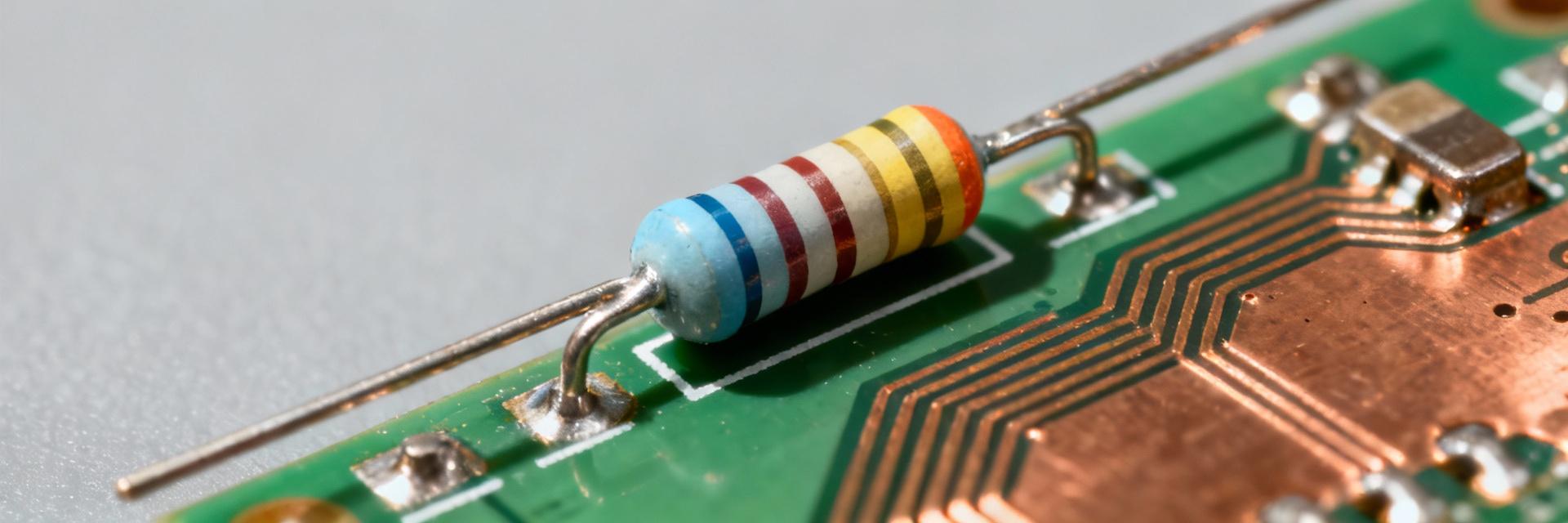
    The F3L600R10N3S7FBPSA1 delivers top-tier power density for three‑level inverter designs — rated for high blocking voltage and hundreds of amperes of continuous current — making it suitable for traction, industrial drives and renewable inverters. This data‑first guide breaks the datasheet into actionable sections: family background, decoded part string, a compact specs table, how to read and verify datasheet numbers, an example 3‑level power stage design, and a bench validation checklist. Background & what the part number means Module family and intended use Point: This module belongs to the high‑power IGBT module class designed for three‑level topologies. Evidence: modules in this class are optimized around series/parallel cell arrangements and integrated half‑bridge layouts. Explanation: three‑level topologies reduce dv/dt and switching stress, yielding lower switching losses and higher efficiency at medium voltage ranges, which benefits traction inverters, large motor drives and PV/energy storage inverters. Decoding the part number and versions Point: The part string encodes voltage class, current capability and package variant; suffixes denote mechanical or sensor options. Evidence: typical decoding maps a leading family code to IGBT generation, numeric groups to voltage/current class, and trailing letters to packaging or added features. Explanation: always check suffixes for thermistor presence, mounting style and busbar options; confirm exact mechanical drawing and ordering code before layout and procurement. F3L600R10N3S7FBPSA1 — Key electrical, thermal & mechanical specs (data analysis / full specs) Electrical ratings & switching specs (spec tables) Point: Key electrical specs determine suitability for system voltage, continuous current and switching performance. Evidence: representative datasheet values (verify against the manufacturer's datasheet for final design): Parameter Typical / Rated Value Test conditions Vces / VCEO 1200 V (blocking) − IC (continuous) 335 A (per module, Tc = 100°C) case temperature specified IC (peak, pulsed) ~1200 A (short pulse) tp, duty per datasheet SOA VCE(sat) (typ) ~1.4–2.0 V at 150–300 A Ig = specified drive Input capacitance Cies variable, tens to low hundreds of nF Vce, f specified Qg / gate charge moderate; design gate driver for 15–20 W switching per device Vge range per datasheet Eon / Eoff (typ) several hundred mJ per pulse (depends on VCC, Ic, VGE) TJ, VCC, IC per datasheet waveform Recommended gate drive Vge_on ≈ +15 V, Vge_off ≤ 0 V; include gate resistor observe dV/dt limitations Explanation: These values are starting points; switching energy and thermal performance are strongly dependent on test circuits and junction temperature. Use the datasheet waveforms and stated test conditions (Tj, Vcc, If) to extract accurate Eon/Eoff and conduction loss numbers for your operating point. Thermal limits & mechanical ratings Point: Thermal resistance and maximum junction/case temps set allowable continuous power. Evidence: typical module limits include Tj(max) ≈ 150°C, recommended Tc(max) for long life ≈ 100°C, and low Rth(j‑c) per IGBT chip to enable effective heat transfer. Explanation: follow recommended mounting torque, use a uniform flat interface and thermal interface material with measured interface resistance. Confirm bolt pattern and footprint against the mechanical drawing and include thermistor or temperature sensing if available in the chosen suffix. How to read the datasheet and verify the specs (method guide: "datasheet" + "specs") Interpreting tables vs. graphs Point: Datasheet tables give absolute maxima and recommended operating points; graphs show performance trends and derating. Evidence: SOA plots, switching energy curves and thermal derating graphs contain the real usable limits for waveform‑dependent events. Explanation: extract usable values by reading curves at your operating Tj and current; note the test circuit used for Eon/Eoff (snubber, stray inductance) and replicate similar measurement setup when validating on the bench. What specs matter for selection Point: Prioritize voltage margin, continuous current rating, switching loss and thermal resistance. Evidence: practical rules: 20–30% voltage margin above DC link, 25–50% current derating depending on cooling, and derate switching energy with rising Tj. Explanation: choose the module with adequate SOA for expected short‑circuit events, and size cooling so case temperature stays within recommended Tc under worst‑case losses. Example system design using F3L600R10N3S7FBPSA1 (case showcase) 3‑level inverter power stage example Point: A compact three‑level inverter using this module targets a 700–900 V DC link with RMS phase currents up to 250–300 A. Evidence: choose switching frequency 2–8 kHz for traction/motor drives to balance switching and conduction losses; gate drive must supply adequate peak current to charge module input capacitance. Explanation: conduction loss estimate Pcond ≈ VCE(sat) × Iavg; for VCE(sat) = 1.6 V and Iavg = 250 A, Pcond ≈ 400 W per conducting device; include switching losses from Eon/Eoff at your Vdc and current to compute total dissipated power per module. Thermal management, layout & protection tips Point: Effective cooling and layout reduce thermal gradients and stray inductance. Evidence: use wide, short busbars or direct copper bus, minimize loop area between DC link and inverter bridge, and choose liquid cooling for sustained high power or forced‑air with large heatsinks for intermittent loads. Explanation: add desaturation detection, fast short‑circuit sensing, and temperature monitoring at the case; size heatsink so case temperature stays below the datasheet recommended Tc under worst‑case power dissipation plus a safety margin. Design validation & deployment checklist (action suggestions) Bench tests and key measurements Point: Validate electrical and thermal behaviour stepwise on the bench. Evidence: core tests—insulation and continuity, gate drive verification, static VCE(sat) and leakage at defined Tj, switching loss measurement with the datasheet test circuit, thermal rise under controlled current. Explanation: run switching tests at representative Vcc and Ic, log waveforms and temperatures; pass/fail criteria should be based on staying within datasheet SOA, acceptable VCE(sat) increase and stable thermal response over test duration. Reliability & safety verification before field deployment Point: Accelerated and in‑system tests reduce field failures. Evidence: perform thermal cycling, humidity exposure, vibration (if applicable), and long‑run endurance at elevated case temperature. Explanation: finalize protection thresholds (desat, overcurrent, overtemperature) and set up runtime logging for case temperature, junction estimates and current spikes to enable early detection of degradation in the field. Summary The module provides a high‑voltage, high‑current three‑level IGBT solution; confirm rated voltage and continuous current on the manufacturer's datasheet before system selection to ensure electrical margin and SOA compliance. Key specs to extract are Vce/VCEO, continuous and pulsed IC ratings, VCE(sat), gate charge, Eon/Eoff with test conditions, plus Rth(j‑c) and Tj/Tc limits; use those numbers to size cooling and gate drivers. Validate on the bench with the datasheet test waveforms: measure conduction and switching losses, verify thermal rise under load, exercise protection features and perform environmental stress tests prior to deployment. Frequently asked questions What are the most important datasheet specs to check for a high‑power inverter module? Check blocking voltage, continuous and peak current ratings, VCE(sat) and its temperature dependence, switching energies with stated test conditions, thermal resistances Rth(j‑c), and maximum junction/case temperatures. These determine electrical margins, cooling needs and protection thresholds for reliable operation. How should switching energy and conduction losses be validated against datasheet specs? Replicate the datasheet test circuit (Vcc, Ic, gate drive waveform, stray inductance) and measure Eon/Eoff and VCE(sat) under the same Tj. Compute conduction losses Pcond = VCE(sat) × Iavg and combine with switching losses at intended switching frequency to size heatsinking and confirm thermal limits. Which thermal management checks are necessary before field deployment? Perform steady‑state thermal rise tests at maximum expected power, thermal cycling for reliability, and assess case‑to‑heatsink interface resistance. Verify that case temperature stays below recommended Tc under worst‑case load plus safety margin, and enable runtime monitoring of case/estimated junction temperature.