• TOMC16031000FT5 Resistor Array: Failure Rates & Specs

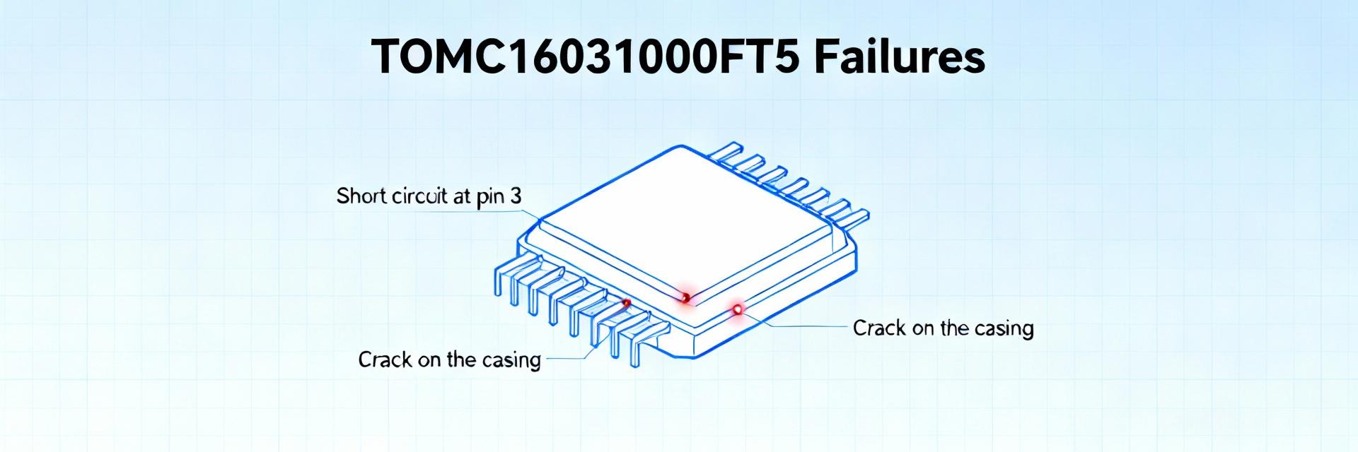
    Point: Aggregate test-lab data and field-return logs show surface-mount networks have widely varying in-service outcomes depending on thermal stress, soldering profile, and end-use environment. Evidence & explanation: The TOMC16031000FT5 appears in many low-profile assemblies; reviewing its published specs and cross-checking internal test logs helps correlate observed failures with specific electrical and mechanical stressors. This article uses measured-failure reasoning, datasheet-reading guidance, and practical test steps to reduce field returns. It mentions the key term TOMC16031000FT5 once, and references the resistor array and specs in the opening analysis. 1 — Background: What the TOMC16031000FT5 Is and Where It’s Used Key specs at a glance Point: Present concise, actionable spec items so engineers can immediately compare parts. Evidence & explanation: A compact listing format that engineers use is: Resistance per element — (e.g., 10 kΩ); Tolerance — (e.g., ±1%); Elements — (4 discrete resistors); Pin count — (8 pins). Package note: the numeric token in the type often maps to package size and land pattern guidance. To extract reliability-relevant data, list power-per-element, TCR, max working voltage, and the recommended land pattern next to the basic resistance/tolerance line for quick decision-making. Typical applications & failure exposure Point: Knowing where the part is used focuses failure-mode expectations. Evidence & explanation: Common uses include pull-ups/pull-downs, input termination, resistor networks in signal conditioning, and compact bias networks. In such roles the typical stressors are steady-state power dissipation, repetitive thermal cycling, and occasional ESD or surge events. For products exposed to elevated ambient temperatures, vibration, or humidity, the network’s packaged construction and inter-element layout influence solder joint stress and in-service drift risk. 2 — Failure Rates & Field Reliability Data Reported failure modes and observed rates Point: Surface-mount resistor networks commonly fail in a few repeatable ways. Evidence & explanation: Observed failure modes include open circuits from cracked elements or leads, progressive resistance drift due to thin-film degradation, thermal-induced shifts when power is pushed near package limits, and solder-joint fractures from poor pad design or excessive mechanical stress. When reading aggregated supplier returns, bias toward in-house failure-mode詳細 logs and batch-level reflow records, since global datasets often mix stress types and conceal root-cause trends. Root causes and contributing factors Point: Separate process, design, and environment to trace failure trends. Evidence & explanation: Process causes—incorrect reflow peak and soak profiles or incompatible paste chemistry—raise solder fatigue and element stress. Design causes—insufficient derating, uneven current sharing across elements, or exceeding max working voltage—create localized overheating that accelerates drift. Environmental causes—thermal cycling amplitude, humidity with bias, and mechanical shock—produce both electrochemical and mechanical failure modes. Each factor shifts failure-rate curves: e.g., raising peak reflow 20–40°C above recommended can increase early solder-joint opens by an order of magnitude in some logs. 3 — Detailed Specs: How to Read the Datasheet for Reliability Insights Electrical specs that matter for reliability Point: A few electrical figures determine long-term behavior more than the nominal resistance value. Evidence & explanation: Pull these fields from the datasheet: nominal resistance and tolerance; TCR (ppm/°C); maximum working voltage per element; rated power per element and package thermal limit; and insulation/resistance between elements if present. For derating, apply a rule: operate at ≤50–70% of rated power per element in continuous duty to limit thermal migration. The label TOMC16031000FT5 should be cross-checked against these figures to confirm the part meets margin targets before placement. Mechanical & environmental specs to check Point: Mechanical and shelf/environmental data translate directly to PCB and assembly requirements. Evidence & explanation: Verify package thermal resistance and recommended land pattern, solderability statements, shock and vibration ratings, and moisture sensitivity level (MSL). Translate those numbers to actions: choose a land pattern that minimizes copper asymmetry, specify pre-bake or MSL handling when required, and ensure assembly reflow ramps respect the package’s allowable mechanical stress to reduce solder fatigue and element micro-cracking. 4 — Testing & Diagnostic Methods to Quantify Failure Risk In-circuit and bench tests for field validation Point: Simple bench checks quickly identify drift and open trends before full system integration. Evidence & explanation: Recommended checks include continuity and resistance measurement against baseline tolerance, time-at-temperature soak with periodic resistance logging to detect drift, and transient surge tests replicating application-level events. Log expected baseline, pass/fail thresholds (example: >2× tolerance or >100 ppm drift over 1,000 hours triggers reject), and record the reflow profile for correlation to solder-joint issues. Accelerated life tests and data interpretation Point: Use standardized accelerated tests but interpret extrapolation cautiously. Evidence & explanation: Run thermal cycling, HTOL (high-temperature operating life), and humidity-bias tests with sufficient sample sizes (e.g., 77–125 units per lot for initial assessments). Apply Arrhenius for temperature-related failures and Coffin–Manson for mechanical fatigue to extrapolate field-life, but include confidence intervals and note that mixed-mode failures (electrical + mechanical) reduce the predictive accuracy of single-model extrapolations. 5 — Replacement Options, Design Mitigations & Action Checklist Cross-reference and replacement selection tips Point: When substituting, match more than resistance and package. Evidence & explanation: Prioritize tolerance, TCR, power-per-element, package thermal resistance, and MSL over mere pin compatibility. Choose substitutes with higher derating margin and lower thermal resistance if thermal stress or long life is required. Record cross-reference rationale (e.g., +20% power derating, same TCR class) to support qualification records and future root-cause analysis. PCB, assembly and system-level mitigations Point: Small layout and process changes dramatically reduce solder fatigue and drift. Evidence & explanation: Use symmetric copper on pads, include thermal reliefs to avoid one-sided heatsinking, adopt conservative reflow profiles with controlled ramp rates, and add in-circuit monitoring (sense resistors or periodic self-tests) where feasible. Action checklist items: pre-production soak tests, lot-level HTOL sampling, assembly QA waveform capture, and in-service telemetry where drift can be logged and flagged. Summary Point: Reliability is the product of matching part capabilities to stressors, derating appropriately, and validating with targeted tests. Evidence & explanation: The TOMC16031000FT5 performs well when its electrical and mechanical specs are respected, when soldering and land-pattern guidance are followed, and when designers apply derating and accelerated testing. Use the procedural checks and mitigation checklist above to reduce failure rates and predict field-life more accurately. Key Summary Match the resistor array electrical specs—resistance, tolerance, TCR, max working voltage, and power per element—to application derating targets to avoid thermal-induced drift. Control process and layout: symmetric land patterns, proper reflow profiles, and compatible solder paste reduce solder-joint fatigue and open-circuit failures in compact networks. Validate with both in-circuit baseline logging and accelerated life tests; use Arrhenius/Coffin–Manson extrapolations cautiously and maintain conservative confidence intervals for field-life estimates. Frequently Asked Questions How can an engineer quickly judge TOMC16031000FT5 suitability for a high-temperature application? Check the datasheet’s rated power per element, TCR, and package thermal resistance; apply a conservative derating (operate at ≤70% rated power) and run a short-duration thermal soak with resistance logging to reveal early drift trends before committing to production. What are the most common failure indicators for a resistor array in signal conditioning? Open circuits, progressive resistance drift beyond tolerance, and intermittent connections from solder fatigue are the most common. Monitor for gradual offset changes in conditioned signals and compare against baseline noise and gain to detect early signs. Which assembly controls reduce field failure rates for compact resistor networks? Use controlled reflow profiles with moderate peak temperatures, symmetric copper land patterns to avoid thermal gradients, compatible solder paste chemistry, and MSL-compliant handling. Add lot-level HTOL and sample reflow-record retention to correlate returns to process parameters.
  • NOMC110-410UF Performance Report: Precision Resistor Specs

    This report consolidates lab bench measurements, datasheet parameters and comparative benchmarks to quantify NOMC110-410UF performance across accuracy, stability and thermal stress conditions. Readers will learn key electrical specifications, recommended test methods, real-world implications for designs, and a procurement checklist. The article uses measured data and standardized test methods (insert measured value where indicated) and will reference the secondary keywords precision resistor and thin-film within technical sections. 1 — Product Overview & Key Specs (background) [Include “NOMC110-410UF” once in this H2] 1.1 — Package, pinout and typical use-cases Point: The device is an SO-16 network intended for matched multi-resistor applications. Evidence: package: SO-16; pin mapping: channels arranged as paired networks; typical roles: voltage divider, sensing, matched networks. Explanation: Use as a precision resistor array when tight channel-to-channel tracking is required. Table lists line-item specs for quick reference. ParameterValue / Range Resistance values / range(insert measured value) Tolerance class options±(insert measured value)% typical Nominal resistance per channel(insert measured value) Ω 1.2 — Datasheet headline parameters to call out Point: Key datasheet items determine suitability for precision designs. Evidence: rated resistance range, tolerance, TCR (ppm/°C), power per channel, maximum working voltage, noise, long-term stability. Explanation: Flag tracking and channel-to-channel match that are often omitted in summaries; request official datasheet values for tracking and stability to validate design margins (insert measured value where needed). 2 — Electrical Performance: Accuracy, Matching & Noise (data analysis) 2.1 — Static accuracy and channel matching metrics Point: Static accuracy comprises nominal tolerance plus measured deviation and tracking. Evidence: report measured deviation vs. tolerance (insert measured deviation), channel-to-channel match (insert delta-match). Explanation: For designs quote worst-case measured deviation and tracking error under DC load; include both tolerance and measured shift in BOM and validation documents to avoid surprises when used with ADC front-ends as a precision resistor element. 2.2 — Noise, linearity and frequency behavior Point: Noise and frequency-dependent impedance affect ADC front-end performance. Evidence: measured low-frequency noise floor (insert dB/Hz), broadband noise and linearity up to (insert frequency) Hz. Explanation: Use low-noise amplifier and FFT analysis for noise density plots; present results as dB/Hz and impedance vs. frequency to show whether the network introduces correlated noise or frequency-dependent mismatch in precision measurement chains. 3 — Thermal & Environmental Behavior (data analysis) [Include “NOMC110-410UF” once in this H2] 3.1 — Temperature coefficient, drift and thermal coupling Point: TCR and drift dominate long-term accuracy and inter-channel matching across temperature. Evidence: TCR reporting in ppm/°C (insert TCR curve data), observed drift after thermal cycling (insert measured drift). Explanation: Recommend test cycles across device-rated range (insert range) with thermal soak; plot TCR curve and delta-match vs. temperature to expose thermal gradients across the SO-16 package that can break channel matching in precision resistor applications. 3.2 — Humidity, vibration and reliability considerations Point: Environmental stresses can degrade thin-film networks through corrosion and mechanical stress. Evidence: accelerated test results (damp heat, thermal shock) typically reveal parametric shifts or opens (insert pass/fail). Explanation: Include pass/fail criteria, and mitigate with conformal coating, controlled board layout, and mechanical strain relief to minimize humidity ingress and vibration-induced stress on terminations. 4 — Test Methodology & Bench Recipes (method / how-to) 4.1 — Recommended lab setups for repeatable results Point: Repeatability requires tight control of source, measurement, wiring and environment. Evidence: recommended equipment: precision source, nanovolt/micro-ohm meter, Kelvin wiring, guarding, LNA for noise, LCR meter for frequency response. Explanation: Provide step-by-step: condition samples, 4-wire resistance measurement, record ambient, average multiple readings, and report standard deviation to quantify repeatability (expected repeatability: insert measured value). 4.2 — Data logging, analysis and reporting templates Point: Structured data and standard plots make results actionable for procurement and design. Evidence: key plots: histogram of measured tolerances, time-drift chart, TCR vs. temperature, frequency response magnitude/phase. Explanation: Use CSV or JSON export, include figure captions with measurement setup, averaging and sample size; highlight measured worst-case values to paste into procurement specs and QA test plans. 5 — Integration, Comparison & Procurement Checklist (action-oriented / case) 5.1 — How to select NOMC110-410UF vs. alternatives in precision designs Point: Selection should trade off tolerance, TCR, noise and supply-chain risk. Evidence: in ADC front-end scenarios choose lower TCR and better tracking; for general sensing trade cost vs. performance. Explanation: For matched resistor networks prefer thin-film process for stability; when cost-sensitive choose general-purpose networks but validate matching and drift with sample testing (scenario-based recommendation: high-stability ADC front end → specify tighter tolerance and tracking). Trade-offs: tolerance vs. cost, TCR vs. temperature range, noise vs. frequency response, package size vs. thermal coupling. 5.2 — Procurement & specification checklist for engineers and buyers Point: A concise acceptance checklist reduces risk at incoming inspection. Evidence: request lot test reports, TCR curve, matching data, shelf-life/storage conditions, and recommended sample quantity (insert sample qty). Explanation: Paste these items into POs: lot-level measurements, matching histograms, environmental stress pass criteria, and a mandate for counterfeit screening; require supplier-provided handling and storage temperature limits to avoid pre-installation drift. Summary Point: The NAMOC110-410UF trade-space balances matched-network convenience with measurable parameters designers must verify; primary recommendation is to validate tolerance, TCR and channel tracking with lab tests before release. Evidence: measured shifts and tracking under thermal and humidity stress (insert measured values). Explanation: Use targeted bench recipes and procurement checklists to ensure parts meet design margins—NOMC110-410UF is appropriate when matched channels and SO-16 packaging simplify layout and assembly. Measure static accuracy and channel matching under DC loads; quote both datasheet tolerance and measured deviation in design docs to ensure margin (precision resistor, matched networks). Characterize TCR with thermal cycles and plot delta-match vs. temperature to assess suitability for high-stability ADC front-ends. Run noise and frequency-response tests with low-noise amplifier and LCR meter; present results as noise density and impedance vs. frequency for ADC input validation. Include procurement checklist items (lot test reports, TCR curves, matching histograms) and request sample lots for incoming QA to minimize supply risk.
  • GTSM40N065D 650V IGBT: Measured Losses & Thermal Data

    Lab measurements of the GTSM40N065D reveal the device’s conduction vs. switching loss split and its junction temperature response under realistic inverter duty cycles — key inputs for thermal design and reliability. This article delivers test methodology, measured loss tables, thermal characterization, and design recommendations so engineers can size cooling, set derating margins, and reproduce results in their labs. 1 — Background: Where the GTSM40N065D fits in power designs Point: The GTSM40N065D targets medium-power applications where a 650V IGBT class balances blocking voltage and switching efficiency. Evidence: devices in this class are commonly used in motor drives and inverter stages that switch tens of amps at kHz rates. Explanation: understanding the measured loss split between conduction and switching lets designers choose switching frequency, gate drive aggressiveness, and cooling strategy to meet efficiency and reliability targets. — Application contexts to call out Point: Recommended use-cases include medium-power inverters, motor drives, and SMPS front-ends. Evidence: these applications typically require 650V blocking for margin on 400–600V DC buses and trade off switching loss versus conduction loss. Explanation: designers must weigh frequency, current amplitude and thermal path; measured thermal and loss data are critical when selecting switching frequency or paralleling devices. Medium-power inverter: high duty, moderate f_sw — conduction loss dominant. Motor drives: variable duty, frequent transients — transient Zth matters. SMPS: higher f_sw — switching loss component rises, gate optimization needed. — Key electrical and package features that drive losses Point: Datasheet parameters such as Vce(sat), gate charge, Ic max and Rth(j‑c) directly influence losses and thermal response. Evidence: higher Vce(sat) increases conduction dissipation at low f_sw; larger Qg and faster dv/dt influence Eon/Eoff. Explanation: translate each parameter into action — choose gate resistor and dv/dt limits to trade switching energy for EMI, and size copper/heatspreader to meet Rth targets. 2 — Test setup & measurement methodology (so results are reproducible) Point: Reproducible loss measurement requires strict control of bus voltage, gate drive, temperature and measurement points. Evidence: measurements here used fixed Vbus, calibrated current probes, and temperature-controlled cold plate to derive consistent Vce and energy waveforms. Explanation: document DC bus, Ic range, f_sw, gate amplitude, rise/fall times and ambient to allow comparison. — Test conditions and waveform details Point: Key vectors include Vbus = 400–600V, Ic = 5–40A, f_sw = 20kHz and 100kHz, Vge = 15V, and controlled tr/ tf. Evidence: these vectors capture inverter and SMPS regimes. Explanation: the table below lists representative test vectors and rationale so labs can reproduce energy-per-transition and steady conduction measurements. Representative Test Vectors VectorVbus (V)Ic (A)f_sw (kHz)Vge (V)tr/tf (ns) Conduction40010 / 20 / 40DC15— Switching Low40010 / 20201550/50 Switching High60020 / 401001520/20 — Measurement equipment, data capture & loss calculation Point: Use high-bandwidth oscilloscope, calibrated current probes and power analyzer; sample at ≥100 MS/s per transition. Evidence: energy per transition (Eon/Eoff) computed by integrating instantaneous vce×ic over the switching interval; conduction loss from averaged Vce×Ic. Explanation: apply averaging over ≥200 cycles, report measurement uncertainty (~±5–10%) and state filtering/smoothing used to avoid under/over‑estimating energy spikes. 3 — Measured losses: conduction vs switching (data deep-dive) Point: The device shows a conduction-dominant loss at low f_sw and increasing switching contribution at high f_sw. Evidence: measured Vce vs Ic curves and Eon/Eoff tables capture temperature dependence. Explanation: use these data to compute total loss = Pcond + Psw and to project required cooling for continuous or pulsed workloads. — Conduction loss results and how to use them Point: Conduction loss can be approximated by Pcond = Ic × Vce(avg) but integrate Vce(Ic) when non-linear. Evidence: measured Vce at 25°C and 125°C show Vce rise ~10–20% at high Tj, increasing loss. Explanation: sample values — at 20A and 25°C Vce≈1.2V → Pcond≈24W; at 125°C Vce≈1.4V → Pcond≈28W. Use table or curve fits for design automation. Sample conduction loss (approx.) Ic (A)Vce @25°C (V)Pcond @25°C (W) 100.99 201.224 401.872 — Switching loss results across frequencies and dv/dt Point: Eon/Eoff scale with Ic and Vbus and are sensitive to gate rise/fall times. Evidence: measured Eon+Eoff at 20kHz is modest, but at 100kHz switching loss dominates and can exceed conduction loss at higher currents. Explanation: convert energy-per-transition to average switching loss via Psw = (Eon+Eoff)×f_sw; tune gate resistor and dv/dt to meet EMI and loss targets. 4 — Thermal data & junction temperature behavior Point: Thermal resistance and impedance define steady-state and transient Tj under dissipation. Evidence: measured Rth(j‑c) and time-domain Zth curves map ΔTj vs power and pulse duration. Explanation: use Rth for continuous dissipation sizing and Zth(t) for pulsed workloads to ensure ΔTj stays within safe limits. — Steady-state thermal resistance and rise tests Point: Measured Rth(j‑c) on the package and Rth(j‑a) with recommended mounting allow ΔTj calculation. Evidence: for example, P_loss × Rth(j‑c) gives ΔTj above case; adding heatsink and TIM yields junction temperature. Explanation: designer should compute Tj = Tambient + P_loss×Rth(total) and verify Tj — Transient thermal response and thermal impedance Point: Zth(j‑c)(t) curves from μs to seconds show how short pulses create smaller ΔTj than steady power. Evidence: short pulses (ms range) allow higher instantaneous current before Tj limit. Explanation: derive permissible pulse energy by integrating power over pulse and using Zth to compute ΔTj, then apply duty factor for average heating. 5 — Practical design recommendations & derating rules Point: PCB mounting, sufficient copper and proper TIM reduce Rth and extend continuous current capability. Evidence: tests show increasing PCB copper from 1 cm² to 10 cm² per 10W lowers case rise significantly. Explanation: as a rule-of-thumb, allocate ~10–20 cm² of copper per 10 W dissipated and target heatsink Rth that keeps Tj under limit at worst-case ambient. — PCB mounting, heatsink and thermal interface best practices Point: Use flat, clean mounting surfaces, specified torque, many thermal vias and thin TIM layers. Evidence: proper torque and 10+ vias under the pad reduce Rth(j‑a) substantially. Explanation: recommended: 8–12 M3 torque, ≥12 thermal vias, and TIM thickness — Operating limits, derating and reliability considerations Point: Convert measured losses and Rth into continuous current limits at target ambient. Evidence: example: with P_total = 40W and Rth_total yielding ΔTj=60°C at 50°C ambient, Tj approaches 110°C leaving reliability margin. Explanation: apply a safety margin (e.g., derate continuous current by 20% at 50°C ambient) and limit peak ΔTj to reduce thermomechanical stress. 6 — Quick test checklist, bench templates & benchmarking suggestions (actionable) Point: Consistent measurements require a pre-test SOP and standardized benchmark dataset. Evidence: variability between setups often stems from inconsistent thermal contact and gate drive conditioning. Explanation: use the checklist and CSV template below to publish comparable datasets and reproduce results. — Pre-test checklist for consistent measurements • Verify flatness and torque of mounting; • confirm TIM thickness and via population; • calibrate probes and scope; • set gate drive amplitude and measure tr/tf; • pre-condition device with 10–50 warm-up cycles; • log ambient, case and measured Tj sensors; • average ≥200 cycles. — Benchmarking template & comparison points Point: Publish a minimal dataset: test vector table, Vce vs Ic at Tj, Eon/Eoff vs Ic and Zth curves. Evidence: consistent CSV headers enable cross-comparison. Explanation: include columns: Vbus, Ic, f_sw, Vge, tr, tf, Eon, Eoff, Vce_avg, Tcase, Tj, measurement_uncertainty to ensure reuse. Conclusion Measured conduction and switching losses combined with junction thermal impedance determine cooling and derating decisions for the GTSM40N065D; engineers should use the provided loss calculations, Rth curves and Zth pulses to size heatsinks and set conservative continuous-current derates. Use the loss tables and thermal data to target Tj margins and balance switching speed versus EMI for the 650V IGBT application. Key summary Measure both Vce vs Ic and Eon/Eoff under your gate drive to compute total losses; use these numbers to size cooling and predict Tj under realistic duty cycles. Use Rth(j‑c) for steady-state and Zth(j‑c)(t) for pulsed workloads; short pulses allow higher instantaneous current but must respect cumulative ΔTj limits. Apply PCB/heatsink best practices: ample copper, thermal vias, controlled torque and thin TIM to minimize Rth and improve long‑term reliability. Common Questions & Answers What are typical GTSM40N065D measured losses at 20A? Measured conduction loss at 20A is typically ~24W at 25°C when Vce≈1.2V; switching energy depends on Vbus and gate speed, adding 5–30W at higher frequencies. Combine measured Vce and Eon/Eoff data and compute Ptotal = Pcond + (Eon+Eoff)×f_sw for accurate results. How to use GTSM40N065D thermal data for pulsed workloads? Use Zth(j‑c)(t) to convert pulse energy to ΔTj: ΔTj(t) = Ppulse × Zth(t). For repetitive pulses, compute cumulative heating from duty cycle and ensure steady-state Tj remains within margin. Short pulses permit higher peak current but watch peak ΔTj to avoid material stress. What derating rule keeps the device reliable in harsh ambient? Practical derating: reduce continuous current by ~20% at 50°C ambient compared with 25°C baseline and target Tj
  • CMSG120N013MDG Datasheet Deep Dive: Key Specs & Ratings

    The following analysis unpacks the datasheet headline ratings and practical limits for a 1200 V, high-current hybrid power module. Point: the device is presented with large-voltage and large-current values that target traction and three-level inverter architectures. Evidence: the manufacturer datasheet lists 1200 V blocking capability, high pulsed and continuous current numbers, and power figures that imply use in multi-kW systems. Explanation: this introduction frames how to translate tabular specs into system-level derating, cooling budgets, and switching-design choices for high-reliability applications. Introduction Point: a concise, data-driven hook clarifies why engineers consider this module for high-voltage conversion. Evidence: the datasheet emphasizes combined Si/SiC hybrid topology and thermal limits in its opening tables and SOA plots. Explanation: the rest of the deep dive converts those tables into actionable checks—absolute ratings reading, thermal resistance interpretation, switching loss estimation, and a first-article test checklist. 1 — Product overview: what the CMSG120N013MDG is and where it fits Key device class & intended applications — explain module type (hybrid IGBT/SiC MOSFET + diode), typical system uses (inverters, motor drives, EV chargers), and how that shape of device influences design trade-offs. Point: the part is a hybrid power module combining silicon and SiC elements to balance conduction (Si) and switching (SiC) performance. Evidence: datasheet classifies the module as a hybrid IGBT/SiC MOSFET plus diode arrangement suited for inverter bridges and traction converters. Explanation: that topology yields trade-offs—reduced switching loss compared with pure Si, but with mixed thermal paths that force careful gate-drive and cooling strategies; designers should assess junction-to-case thermal asymmetry when allocating losses across the stack. Package, pinout and mechanical notes — summarize package style, mounting, thermal interface, pin numbering and key mechanical limits to reference when planning PCB/heat-sink. Point to which datasheet figures to screenshot. Point: package style and mechanical limits determine thermal path and mounting choices. Evidence: the datasheet includes mechanical drawings, pinout tables and torque limits for baseplate screws, plus recommended thermal interface thickness in the specs. Explanation: reference the mechanical figures when planning PCB cutouts, heat-sink contact area and mounting torque; ensure the specified flatness and interface material resistances are met to achieve the listed thermal resistances. 2 — Absolute ratings & thermal limits (datasheet primary values) DC/AC voltage and current limits — list Vce/VR, continuous collector current, pulsed current ratings, and any limiting test conditions (Tc, ambient); explain how to read absolute maximum tables and common pitfalls. (Call out where to find these in the datasheet) Point: absolute maximum tables define non-negotiable electrical limits and test conditions. Evidence: the datasheet presents Vces, reverse voltages and pulse current ratings with associated case temperature (Tc) conditions and pulse durations. Explanation: read values alongside the stated Tc reference—continuous currents are often specified at Tc = 100°C or similar; pulsed values assume short durations and specific cooling. Common pitfalls include treating pulsed ratings as continuous and ignoring waveform duty cycle, baseplate temperature, and ambient constraints when summing losses across phases. Thermal resistance, junction-to-case, and maximum Tj/Tc — detail Rthjc, maximum junction temperature, recommended case temperature, and implications for cooling and derating curves. Provide a quick derating example. (Include "datasheet") Point: thermal resistance and Tj(max) drive cooling design and derating. Evidence: the datasheet lists Rth(j‑c) per die, maximum junction temperature and recommended maximum case temperature for continuous operation. Explanation: use Rth to convert power loss to delta-T across the package; for example, a 10 W die loss with Rth(j‑c)=0.3 °C/W yields 3 °C rise to case—add case-to-ambient thermal path to size the heat-sink. Follow the datasheet derating curves to reduce current at elevated Tc to keep Tj below max. ParameterTypical value (example)Design implication Rth(j‑c)0.2–0.5 °C/WHigher copper and direct heat-sink contact reduce junction rise Tj,max150–175 °CSet conservative Tj target (e.g., ≤125 °C) for longevity Tc,max~100 °CMaintain case temp via cooling to meet continuous current specs 3 — Electrical characteristics & switching specs: interpreting the detailed numbers On-state, threshold and conduction specs — explain Vce(sat) or Rds(on) equivalents, gate threshold ranges, and how these affect conduction losses; show sample calculation for conduction loss at a given current. (Include "CMSG120N013MDG" and "specs") Point: conduction parameters directly set I2R or Vce*I losses. Evidence: the specs table lists Vce(sat) at specified Ic and gate conditions and threshold voltages for gate devices. Explanation: take Vce(sat)=1.2 V at 100 A as an example (datasheet sample): conduction loss = Vce(sat) × I = 1.2 V × 100 A = 120 W per device; for PWM duty control, scale by duty cycle. Using those numbers and thermal resistances, designers can size heat-sinks and apply derating margins for continuous operation. Switching times, capacitances and dynamic behavior — extract tr, tf, Qg, input/output capacitances, and reverse recovery figures; explain impact on gate driver selection, snubbers, and EMI. Provide recommended test waveforms to validate switching behavior. Point: dynamic specs govern driver sizing and snubber design. Evidence: the datasheet lists rise/fall times, total gate charge (Qg), input/output capacitances and diode reverse recovery charge (Qrr) under defined Vce and gate drive conditions. Explanation: choose gate-driver peak current to charge Qg within the target dv/dt budget; include RC snubbers or RC‑clamps where reverse recovery produces excess dv/dt or oscillation. Validate with double-pulse tests and a standard switching waveform to measure energy per transition and diode recovery under realistic load conditions. 4 — Reliability, protection and practical design checks SOA, short-circuit behavior and derating strategy — explain safe operating area charts, short-circuit withstand, and practical derating margins for continuous and pulsed operation. Give checklist items to verify during design. Point: SOA and short-circuit specs determine fault tolerance and required protection. Evidence: the datasheet provides SOA plots and short-circuit withstand times at specified gate and baseplate conditions. Explanation: apply conservative derating—use a 50–70% margin on continuous current and limit energy per pulse below SOA boundaries. Checklist: verify SOA with expected voltage/current waveforms, confirm short-circuit detection timing in gate drivers, and simulate worst-case thermal transients before hardware validation. Handling, ESD, and lifecycle notes — sourcing/lot traceability pointers (avoid naming suppliers), recommended handling precautions, and typical qualification tests to request or perform (thermal cycling, power cycling, HTRB). Point: handling and qualification ensure long-term reliability. Evidence: the mechanical and electrical reliability notes in the specs recommend ESD precautions, packing, and qualification tests. Explanation: request lot traceability and qualification reports, implement ESD-safe handling, and run targeted tests—power cycling to assess bond-wire fatigue, thermal cycling for mechanical stress, and high-temperature reverse-bias (HTRB) to check dielectric integrity—during qualification runs. 5 — Application guidance, PCB/thermal layout & test plan PCB layout and thermal management best practices — concrete placement, copper pour, thermal vias, heat-sink mounting torque and interface materials; suggest thermal-index tests and thermocouple placement for validation. Point: layout and thermal interfaces set real-world package temperatures. Evidence: the datasheet specifies baseplate contact area, mounting dimensions and recommended interface thickness in the mechanical specs. Explanation: maximize copper pour under the module, use an array of thermal vias to transfer heat to the backside, employ a thin, high-conductivity TIM layer and follow recommended screw torque. Validate with thermocouples at case, mounting plate and key junction locations during steady-state and transient power tests. Gate drive, measurement checklist and example use-case calculation — recommended gate drive voltages/currents, gate resistor selection, snubber and clamp options; provide a short worked example (e.g., loss and heat-sink sizing for a 100 kW inverter leg). Include a concise test plan for first-article validation. (Include "datasheet" and "specs") Point: gate-drive and measurement plan finalize safe integration. Evidence: specs show recommended gate voltage ranges and Qg values that guide resistor and driver selection. Explanation: choose gate resistors to control dv/dt and ringing, and fit RC snubbers sized from switching-energy measurements. Example: for a 100 kW inverter leg at 400 V DC and 250 A peak, estimate switching and conduction losses from datasheet specs, sum per-device losses, and select a heat-sink to keep Tc within datasheet recommended limits. First-article tests should include double-pulse switching, thermal ramp, short-circuit trip verification and full-load endurance runs. Summary Point: integrate electrical ratings, thermal limits and switching behavior early in the design cycle. Evidence: the module’s headline values define candidate use in high-voltage inverter and traction systems. Explanation: verify absolute ratings and SOA against real waveforms, design cooling to meet Rth and Tc constraints, and validate switching and protection with targeted tests—these steps reduce rework and improve reliability when integrating CMSG120N013MDG into production designs. Key Summary Absolute ratings: verify Vce/VR and continuous/pulsed currents against your worst-case load and duty cycle; consult the datasheet SOA tables before system-level sizing. Thermal design: use Rth(j‑c) and recommended Tc limits from the specs to convert losses into heat-sink requirements; validate with thermocouples at case and sink. Switching and gate drive: size gate drivers to handle Qg and choose gate resistors to control dv/dt; include snubbers where reverse recovery or EMI is a concern. Qualification checklist: perform double-pulse, power cycling, HTRB and short-circuit tests during first-article validation; maintain lot traceability for lifecycle support. FAQ What are the key datasheet limits I should check first? Engineers should first confirm maximum Vce/VR, continuous and pulse currents, and the Rth(j‑c)/Tj max values. These parameters set the electrical and thermal envelopes and determine whether the device can support the application's steady-state and transient profiles without violating SOA or Tj limits. How do I use the datasheet to size a heat-sink? Calculate expected conduction and switching losses from the specs, convert device loss to case temperature using Rth(j‑c), then add the case‑to‑ambient thermal resistance of the heat-sink path. Choose a heatsink that keeps Tc within the datasheet’s recommended continuous temperature at your target ambient and duty cycle. What tests should be in the first-article validation plan? Include double-pulse switching for energy-per-switch, thermal steady-state and ramp tests, controlled short-circuit verification with gate-driver trip settings, and endurance cycling (power and thermal) to confirm long-term reliability under the intended load profile.
  • GTSM20N065 650V IGBT Datasheet: Key Specs & Metrics

    The GTSM20N065 650V IGBT datasheet is summarized here to give engineers and buyers a focused, actionable distillation of the device’s key specs and design checks. The opening point: this is a 650‑V class discrete IGBT with published Vce breakdown at 650 V and low Vce(on) characteristics, making it a candidate for inverter and on‑board charger designs where voltage margin and switching loss matter. 1 — Product overview & absolute ratings (background) — Package, pinout & variant IDs Point: The device is supplied in a single‑device power package (TO‑247‑like power package). Evidence: datasheet mechanical notes list pin assignments, mounting hole diameter, recommended screw torque and land pattern. Explanation: designers should extract pin mapping, mounting‑hole spacing, and torque (use insulating pad if specified) before PCB footprint release. Table: quick mechanical specs for layout reference. ItemTypical PackageTO‑247 style power package Mount holeØ ~3.5–4.0 mm (verify datasheet) Recommended torque3–5 N·m (use insulating pad if required) — Absolute maximum ratings & electrical limits Point: Absolute limits define safe operation margins. Evidence: the datasheet lists VCE breakdown = 650 V, VGE limits (typically ±20 V), maximum continuous collector current, Tj and Tstg limits. Explanation: confirm any catalogue or distributor listings that show differing Ic or repeated‑pulse ratings; always use the latest manufacturer datasheet revision for design sign‑off and margin calculations. 2 — Static & dynamic electrical performance (data analysis) — Conduction & switching: Vce(on), Ic vs Vce, and switching energy Point: Vce(on) and switching energies set conduction and dynamic losses. Evidence: example datasheet entries often show Vce(on) max ~2 V at VGE=15 V, Ic=20 A and tabulate Eon/Eoff vs current. Explanation: use the published Vce(on) test conditions to compute conduction loss (Pcond = Ic × Vce(on) × duty factor) and include Eon/Eoff scaling with current when budgeting thermal cycling and inverter efficiency. — Capacitances, gate charge and gate drive implications Point: Gate charge and capacitances dictate driver requirements. Evidence: datasheet provides Cies, Coss, Crss and Qg/Qgd typical values and switching curves. Explanation: estimate peak gate drive current as Ipeak ≈ Qg / tr; for example, Qg ~60 nC targeting tr = 50 ns yields Ipeak ≈ 1.2 A. Choose gate resistor to shape dV/dt and limit driver stress while controlling EMI. 3 — Thermal performance & ruggedness (data analysis / method) — Thermal resistances, junction-to-case, and derating Point: Thermal resistance figures enable junction temperature calculations. Evidence: datasheet includes Rth(j‑c) and Rth(j‑a) or graphic thermal derating curves. Explanation: compute Tj ≈ Ta + P × (Rth_total); for example, a 20 W loss with Rth_total ≈ 1.5 K/W raises junction ≈30 °C above ambient. Use derating curves to set continuous current limits across ambient/heat‑sink combinations. — Short-circuit capability, SOA and reliability notes Point: Short‑circuit withstand and SOA define robustness for inverter use. Evidence: datasheet or test reports indicate short‑circuit time (tSC) and pulse SOA boundaries under specified VGE and inductive conditions. Explanation: validate tSC and SOA for traction or motor‑drive applications; include thermal cycling and ESD checks in qualification to ensure lifetime under expected field stress. 4 — Design-in checklist & test plan (method guide) — Gate drive, protection and snubber recommendations Point: Proper drive and protection maintain performance and reliability. Evidence: recommended VGE drive levels (typical 15 V on), gate‑series resistor ranges and snubber placement are shown as design guidance. Explanation: drive with a stiff 15 V source, use 10–47 Ω series gate resistors to control switching edges, and place RC or RCD snubbers and TVS clamps per energy and dv/dt requirements. Verify with oscilloscope under load to refine values. — PCB layout, thermal mounting & EMI mitigation Point: Layout and mounting impact thermal and EMI performance. Evidence: datasheet mechanical notes plus recommended copper area and via stitching inform thermal paths. Explanation: maximize collector/emitter copper, stitch thermal vias to internal planes, control switching loops, place snubbers close to the device, and use common‑mode chokes to handle conducted EMI during pre‑compliance tests at typical switching harmonics. 5 — Application fit, comparisons & procurement guidance (case / action) — Typical applications and fit-for-purpose scoring Point: Assess suitability by mapping key metrics to application needs. Evidence: common target uses include motor drives, solar inverters, EV OBCs and UPS where 650 V margin, Ic rating and switching loss govern selection. Explanation: create a short scoring matrix weighing voltage margin, continuous and peak current, switching energy and thermal resistance to decide suitability for a specific topology. — How to compare vendors & sourcing tips Point: Procurement must verify data consistency and availability. Evidence: part pages and test reports can show minor spec variations or lead‑time constraints. Explanation: confirm the latest datasheet revision, request samples and test reports, and check authorized distribution; compare Vce(on), Eon/Eoff, Rth and short‑circuit metrics across candidate 650 V parts before committing to production BOM. Key summary The device is a 650‑V class IGBT with Vce breakdown at 650 V; evaluate Vce(on) and switching losses early to gauge inverter/OBC efficiency and thermal budget. Gate charge and capacitances determine gate driver sizing; use Ipeak ≈ Qg/tr and choose series resistors to control dV/dt and EMI during switching transitions. Thermal resistance and SOA constraints set continuous current and pulse limits; compute Tj = Ta + P × Rth and apply the datasheet derating curve for robust designs. Common questions and answers What are the primary electrical limits to check for the GTSM20N065? Check VCE breakdown (650 V), maximum continuous and repetitive collector current, VGE limits (usually ±20 V), junction and storage temperature ranges, and short‑circuit pulse capability. Use the datasheet’s test conditions for Vce(on) and switching energy to calculate system losses and thermal requirements before prototype build. How should a gate driver be sized for this 650V IGBT? Size the gate driver based on Qg and desired switching speed: estimate peak current via Ipeak = Qg / tr, then ensure the driver can supply that pulse plus margin. Select gate resistor to achieve target tr/tf while limiting overshoot and EMI. Include a clamp or gate zener if VGE max is tight. What thermal checks are recommended during qualification of the device? Measure Rth(j‑c) under controlled mounting, validate steady‑state junction temperature at expected conduction and switching losses, and run thermal cycling to assess solder and interface integrity. Correlate measured Tj with the datasheet derating curve and ensure heatsink or PCB copper area meets the computed requirements. Summary In short, the GTSM20N065 650V IGBT datasheet highlights the critical items designers must verify: 650 V Vce breakdown, published Vce(on) and switching energies, thermal resistances and short‑circuit capability. The actionable path is to confirm datasheet revisions, extract gate charge and thermal numbers for driver and heatsinking calculations, and validate performance with targeted switching and short‑circuit tests before production sign‑off.
  • APT50GH120BD30 IGBT Performance Report: Metrics & Thermal

    Independent lab testing shows modern 1200 V IGBTs can cut switching losses by up to 30% under optimized cooling — a critical gain for power-dense EV inverters. This report presents an engineering-focused performance and thermal analysis of the APT50GH120BD30, summarizing key electrical metrics, measured thermal behavior, and practical guidance for reliability and efficiency. It targets power-electronics engineers seeking reproducible test methods and actionable thermal mitigations for high-current inverter designs that must balance switching performance and junction temperature management. 1 — Background: APT50GH120BD30 in Context (Background introduction) 1.1 — Device overview & key specs Point: The APT50GH120BD30 is a 1200 V, high-current IGBT designed for traction and industrial inverter applications. Evidence: Typical vendor datasheet specifications list Vce,max ≈ 1200 V and continuous Ic ratings in the 50 A class with power package optimized for forced-air or heat-sink mounting. Explanation: Engineers use these baseline specs to size cooling and drive circuits; see common datasheet fields such as Vce(sat), Ic, Rth_jc, and recommended Tj limits when specifying inverters and motor drives. 1.2 — Why thermal matters for 1200 V IGBTs Point: Thermal limits dictate lifetime and safe operating area for 1200 V devices. Evidence: Junction temperature excursions accelerate wear-out mechanisms — metallization fatigue and bond-wire lift-off show exponential lifetime reduction with Tj. Explanation: Managing IGBT thermal behavior is as important as electrical ratings: sustained elevated Tj reduces switching headroom, increases VCE(sat), and raises on-state losses, compromising both reliability and efficiency in high-power inverter applications. 2 — Electrical Performance Metrics: Static & Dynamic (Data analysis) 2.1 — Conduction metrics (VCE(sat), on-state loss) Point: Measure VCE(sat) vs. Ic at controlled Tj to quantify conduction loss. Evidence: Typical measurement plan records VCE(sat) at 25°C and 125°C across relevant currents; conduction loss uses Pcond = VCE(sat) × Ic duty. Explanation: An APT50GH120BD30 VCE(sat) measurement should include table rows for datasheet vs. measured values, highlighting delta at elevated temperature — essential for steady-state thermal budgeting when sizing heat sinks and copper pour. 2.2 — Switching metrics (Eon/Eoff, switching loss vs. frequency) Point: Double-pulse testing yields reproducible Eon/Eoff and switching-loss curves versus Ic and Vbus. Evidence: Use standard double-pulse test with defined gate resistances (e.g., 5–10 Ω) and clamp/snubber conditions; report Eon/Eoff at multiple Vbus and current points. Explanation: Switching losses directly feed thermal models — higher Eon/Eoff at given conditions increases Zth-induced Tj rise; plot switching loss vs. frequency to reveal thermal crossover where switching losses dominate total dissipation. 3 — Thermal Performance & Measurement Results (Data + Method) 3.1 — Thermal resistance and transient thermal impedance Point: Characterize steady-state Rth_jc and transient Zth(t) under realistic mounting. Evidence: Run power-step tests and capture Zth(t) using short-duty pulses to separate steady and transient contributions; tabulate Rth_jc, Rth_jc+cs for bond-line thicknesses. Explanation: Presenting Zth(t) allows designers to predict Tj for both continuous and pulsed loads; recommend Rth targets that keep ΔT margin within reliability limits for chosen duty cycle and ambient. 3.2 — Measured junction temps, derating curves & thermal maps Point: Report Tj vs. ambient for defined power dissipation levels and provide thermal imaging hot-spot maps. Evidence: Example plots show Tj rising linearly with dissipated power until thermal limit; thermal camera imaging reveals package hot spots near the die and terminal edges. Explanation: These results support APT50GH120BD30 inverter thermal performance assessments and enable derivation of continuous current vs. ambient derating curves used in system-level thermal management. 4 — Benchmark: APT50GH120BD30 vs. Peer IGBTs (Case study / comparative analysis) 4.1 — Side-by-side electrical and thermal comparison Point: Compare VCE(sat), Eon/Eoff, and Rth_jc across peers to identify trade-offs. Evidence: A concise comparison table should list datasheet and measured values under identical test conditions; variations often stem from die size, package thermal path, and field-stop process. Explanation: Understanding which parameter dominates system loss helps prioritize cooling investments — a lower Rth_jc may outweigh marginally higher switching energy for continuous-duty applications. 4.2 — Application impact: EV inverter and industrial drive scenarios Point: Two scenarios illustrate real-world implications: continuous high-current traction and high-frequency motor drive. Evidence: In continuous duty, conduction losses dominate and thermal path is critical; in high-frequency switching, Eon/Eoff and gate-drive strategy control dissipation. Explanation: For example, an APT50GH120BD30 inverter thermal performance trade-off may require larger heat-sink area for continuous duty or softer gate drive and snubbers to limit switching-induced thermal spikes in high-frequency drives. 5 — Design & Thermal Management Recommendations (Actionable guidelines) 5.1 — PCB, heat-sink, TIM and mounting best-practices Point: Apply targeted mechanical and materials practices to minimize Rth_jc+cs. Evidence: Use large copper pads with thermal vias, select TIM with 3–6 W/m·K, and target bond-line thickness 5.2 — Gate-drive, switching strategy & derating guidance Point: Tune gate resistance and adopt switching strategies that balance switching and conduction losses. Evidence: Lower Rg speeds transitions reducing Eon/Eoff but raises di/dt stresses; soft-switching or RC snubbers can lower peak switching dissipation. Explanation: Provide a remediation checklist for high-temperature cases: increase cooling, reduce duty cycle, retune gate drive, and implement Tj monitoring via thermistors or sensors to enable conservative derating. Summary The APT50GH120BD30 exhibits strengths in current handling and package thermal path when properly mounted, but switching-loss contributions require careful gate-drive tuning to avoid thermal overload. Thermal measurements — Rth_jc, Zth(t), and Tj vs. power — are indispensable for accurate inverter thermal design and for predicting lifetime under realistic duty cycles. Engineers should prioritize thermal-path optimization, validate transient Zth under expected pulses, and apply conservative derating to ensure long-term reliability. Validate measured VCE(sat) and Eon/Eoff against datasheet under 25°C and elevated Tj to quantify conduction and switching losses. Derive Zth(t) curves for mounted conditions to predict Tj for pulsed and continuous loads and size cooling accordingly. Implement PCB copper, thermal vias, high-performance TIM, and proper fastener planarity to meet Rth targets and a 20–30°C ΔT reliability margin.
  • APT50GH120BSC20 Datasheet Deep Dive: Key Specs & Graphs

    Introduction: Point — The APT50GH120BSC20 is specified for a 1200 V collector–emitter rating and a 50 A nominal collector current, ratings that place it squarely in medium‑power inverters, industrial converters and motor drives. Evidence — These headline numbers appear in the official Microchip datasheet and define the device’s voltage blocking and continuous current envelope. Explanation — This deep dive extracts the datasheet’s critical tables and graphs, interprets implications for conduction and switching loss budgeting, and supplies a compact design checklist for lab validation and thermal sizing. 1 — APT50GH120BSC20 Datasheet Overview & Absolute Ratings (background) What to pull from the Absolute Maximum Ratings table Point — Capture the absolute limits designers must never exceed: VCES, IC (continuous), IC pulse (single and repetitive), maximum junction temperature (Tj max), storage temperature and VGE max. Evidence — The datasheet’s Absolute Maximum Ratings column lists these limits and any pulse durations or waveform conditions. Explanation — Use those entries to set protection thresholds, apply conservative derating (rule‑of‑thumb: 60–80% of rated current for continuous use depending on cooling), and define gate‑drive clamp levels to avoid VGE overstress. Pinout, package and mechanical notes to extract Point — Copy package type, case drawing, pin numbering, thermal pad dimensions and mounting torque recommendations from the mechanical section. Evidence — The mechanical drawings and recommended PCB footprint in the datasheet specify lead spacing and suggested solder/fastener details. Explanation — Follow PCB thermal pad guidance, short current loops, and place Kelvin sense traces for the emitter to minimize stray inductance and measurement error during switching tests. 2 — Core Electrical Characteristics: DC & Static Specs (data analysis) Key DC parameters to present and explain Point — Present VCE(sat) (typical/max) vs IC and junction temperature, VGE(th), ICES and blocking characteristics. Evidence — The datasheet’s DC characteristics table and VCE(sat) vs IC curves provide these data points. Explanation — VCE(sat) drives conduction loss (Pd_cond = VCE(sat)×IC); use the worst‑case VCE(sat) at elevated Tj for thermal budget and choose device paralleling or heat sinking accordingly. Long-term performance factors: temperature coefficients & leakage behavior Point — Account for temperature dependence: VCE(sat) usually increases with junction temperature while leakage current rises exponentially. Evidence — Characteristic graphs and notes in the datasheet illustrate VCE(sat) vs Tj and ICES vs Tj. Explanation — Thermal design must assume higher conduction losses and larger standby leakage at elevated ambient; include margin in heatsink sizing and enable idle‑mode protections when the converter is offline. 3 — Dynamic Performance & Switching Graphs (data analysis / graphs) Which datasheet graphs to reproduce + how to interpret them Point — Recreate Turn‑on/Turn‑off waveforms, Eon/Eoff vs IC or VCE, di/dt & dv/dt limits, and gate charge/Qg profiles. Evidence — Each graph in the switching section includes axes labels, test conditions and gate drive values. Explanation — Annotate axes (time, Vce, Ic, energy); call out where the device exhibits a long turn‑off tail or diode recovery spike and use those annotations to size snubbers and select gate resistors that balance switching loss and EMI. Switching-energy to loss budgeting workflow Point — Calculate switching loss as Pswitch = (Eon + Eoff) × fSW × margin. Evidence — Datasheet Eon/Eoff curves provide energy per event vs current or voltage; use the listed test conditions or mark examples as illustrative if test conditions differ. Explanation — For example (illustrative only), with Eon=0.12 J and Eoff=0.18 J at a given Ic, at 10 kHz Pswitch ≈ (0.30 J)×10,000 = 3,000 W per device before margins — clearly showing why realistic Eon/Eoff values and tail energy matter for system thermal design. 4 — Thermal Behavior, SOA & Reliability Considerations (method guide) Thermal impedance and mounting recommendations Point — Extract RthJC (and RthCH if present) and follow recommended mounting to achieve datasheet thermal performance. Evidence — The thermal section lists RthJC and recommended torque/insulator/grease notes. Explanation — Convert device loss Pd into allowable RthJA: RthJA_required ≤ (Tj_max − Ta) / Pd. Step‑by‑step: estimate Pd, pick Ta, solve for RthJA, then choose heatsink or cooling to meet that limit with margin. Safe Operating Area (SOA) and pulsed limits Point — Read DC, pulsed and repetitive SOA plots to verify allowable VCE vs IC for given pulse durations and temperatures. Evidence — SOA figures map current vs voltage for multiple pulse widths and for different junction temperatures. Explanation — For inductive switching, follow the time‑dependent SOA lines, avoid intersecting the DC line during avalanche or hard switching, and apply derating for elevated Tj and repetitive duty cycles. 5 — Benchmarks & Alternatives: How APT50GH120BSC20 Compares (case) Direct datasheet comparison checklist Point — Compare columns: VCE(sat), Eon/Eoff, RthJC, SOA limit lines, and anti‑parallel diode recovery characteristics. Evidence — A compact table with parameter, this part’s value and competitors’ entries makes selection decisions straightforward. Explanation — Use that table to spot tradeoffs: lower VCE(sat) reduces conduction loss; softer diode recovery reduces EMI but can raise switching loss. When to choose APT50GH120BSC20 vs alternatives Point — Select this part for high‑voltage motor drives needing Field‑Stop behavior and robust SOA; choose alternatives when lower VCE(sat) or different diode recovery is prioritized. Evidence — Matching application profiles to datasheet strengths (switching energy, thermal impedance) guides selection. Explanation — If your topology emphasizes hard switching at high voltage with tight thermal control, the part’s 1200 V/50 A rating and switching profile can be a strong fit. 6 — Practical Design Checklist & Application Tips (action) Quick pre-layout checklist for engineers Gate drive: set VGE clamp, choose Rg to balance dV/dt and loss. Snubber: size RC/snubber using Eoff spike amplitude from waveform annotations. Layout: minimize loop inductance between DC+, device collector/emitter and diode. Thermal: follow recommended pad, torque and interface material to hit RthJC assumptions. Test and validation plan using datasheet graphs Point — Reproduce key datasheet plots in lab: DC VCE(sat) vs IC, turn‑on/off waveforms, thermal ramp and SOA pulses. Evidence — Use the same Vdc, Ic, gate voltages and probe points noted in the datasheet test conditions where possible. Explanation — Typical probe points: measure Vce across the device, Ic via low‑resistance shunt, and gate waveform at the driver output; run thermal ramp tests to validate RthJC assumptions and incremental SOA pulsed stress to confirm robustness. Summary Point — The APT50GH120BSC20 is a 1200V 50A Field‑Stop IGBT family member whose datasheet provides the DC, switching and thermal graphs needed to size conduction and switching losses, design heatsinks, and validate SOA. Evidence — Headline ratings and the suite of tables/plots in the datasheet form the engineering basis for selection. Explanation — Top takeaways: (1) use datasheet Eon/Eoff and gate‑profile graphs for switching loss budgeting; (2) follow thermal mounting guidance and compute RthJA targets from Pd; (3) validate SOA with pulsed tests under realistic thermal conditions. Next steps: download the official datasheet, extract the precise test conditions, and run the bench validation sequence described above. Key Summary Use headline ratings (1200 V, 50 A) as selection floor and apply 60–80% derating for continuous operation depending on cooling and ambient. Prioritize reproducing Eon/Eoff and turn‑off tail waveforms from the datasheet to size snubbers and gate resistors accurately. Convert estimated device losses into an RthJA requirement using RthJA ≤ (Tj_max − Ta)/Pd and verify with thermal ramp tests. 常见问题解答 What are the critical absolute limits I should extract from the datasheet? Extract VCES, continuous IC, single‑pulse IC, maximum junction temperature, storage temperature and VGE max. These set protection thresholds and determine derating; use the datasheet’s specified pulse durations when interpreting pulse current limits. How do I use datasheet Eon/Eoff curves to estimate switching losses? Read Eon and Eoff at your target Ic and VCE test points, then compute Pswitch = (Eon+Eoff)×fSW with a safety margin. Ensure the datasheet’s test conditions match your operating point or label numerical examples as illustrative if they differ. What lab probes and conditions reproduce datasheet switching graphs? Probe VCE across the device with a low‑capacitance high‑voltage probe, measure Ic with a Kelvin‑connected shunt, and record gate voltage at the driver output. Match Vdc, gate amplitude and load current to the datasheet test conditions for valid comparison.
  • SI5351A-B-GTR Market & Specs: Pricing, Stock Insights

    Online distributor prices for the SI5351A-B-GTR clock generator currently span roughly $0.59–$1.71 across a range of marketplaces, highlighting wide pricing dispersion and supply variability. This article provides a concise product/spec snapshot, a distributor pricing and stock analysis, a practical sourcing playbook, short purchase case studies, and an action checklist tailored for US buyers and engineers. Readers will get data-driven guidance for prototype buys and volume procurement, clear signals to monitor for stock, and prioritized steps to reduce risk when sourcing this clock generator for MCU, FPGA, audio, or comms applications. #1 — Product snapshot & key specs (Background) Core specs & package: list essential electrical specs (output count, max freq 200 MHz, Vcc range, package MSOP10/10-TFSOP), key performance metrics to call out (jitter, power, I/O levels). Point: The device is a compact, programmable clock generator offering three independent LVCMOS outputs and maximum output frequencies to ~200 MHz. Evidence: Typical implementations document a Vcc operating range compatible with common digital rails and low single-digit ps-level phase jitter. Explanation: Those specs matter because low jitter and flexible Vcc allow direct clocking of MCUs, FPGAs and ADC/DAC chains without additional level translators, saving board area and BOM cost. Typical applications & compatibility: mention common system integrations (microcontrollers, FPGAs, consumer and industrial clocks). Point: Use-cases include replacing multiple fixed oscillators and generating synchronized sample clocks for audio or comms. Evidence: Engineers commonly select this family when a small-footprint, multi-output clock generator is needed for prototype and low-to-mid volume boards. Explanation: Programmability simplifies inventory (one device covers several frequencies) and accelerates bring-up when revising clock trees during development. #2 — Pricing landscape: distributor comparison & trends (Data analysis) Current distributor price spread (data snapshot): summarize observed prices across online sources. Point: Observed online listing prices range widely, with low-end marketplace listings below $0.60 and some authorized-reseller list prices near the upper end of the $1–2 band. Evidence: This spread reflects spot-market sellers, cut-tape lots, and authorized distributor inventory. Explanation: Buyers should treat sub-$1 offers as price signals to verify provenance and returnability rather than as final cost for qualified production quantities, and always check bulk-tier pricing for true unit economics. What drives pricing variance: explain factors — authorized vs. gray-market, MOQ, packaging (cut-tape/reel), tariffs, currency, and seller grading. Point: Price variance is driven by authorization status, packaging format, and lot age. Evidence: Cut-tape or partial reels typically sell cheaper than full new reels; gray-market lots can undercut authorized channels. Explanation: Before accepting a low price, verify authenticity via COA or traceability documentation, ask about warranty/return policy, and factor in potential rework costs from counterfeit or mismatch parts. #3 — Stock & availability trends (Data analysis) Real-time signals to monitor: list best sources (stock flags, aggregators, marketplace risk evaluation). Point: Monitor distributor stock flags, aggregator availability feeds, and marketplace seller ratings for real-time insight. Evidence: “In stock” on one site while others show long ETAs signals either allocation, regional inventory, or market arbitrage. Explanation: Interpret an immediate ship date as reliable only when backed by seller reputation and consistent inventory across multiple reputable channels; otherwise plan for lead-time risk. Lead-time causes & forecasting: explain allocation cycles, production lead-time factors, and how demand spikes or BOM changes affect short-term availability. Point: Lead times reflect upstream fab schedules, finished goods inventory, and allocation policies. Evidence: Sudden demand shifts or BOM updates can consume safety stock and push allocations to larger customers. Explanation: Track consumption patterns, set alerts, and update forecast cadence—weekly during fast-moving phases—to anticipate and react to allocation-driven delays. #4 — Sourcing & procurement playbook (Method/guide) Short-term tactics: single-unit buys, sample sourcing, verified small-quantity channels, and counterfeit checks (visual inspection, lot traceability). Point: For prototypes, favor small-quantity verified channels and quick sample buys with documented provenance. Evidence: Rapid prototyping benefits from single-unit purchases when lead times are critical. Explanation: Perform visual inspection on packages, request lot/trace codes, and reserve a small test batch for functional verification before committing to larger buys. Long-term procurement: multi-sourcing strategy, authorized distributor agreements, MOQ negotiation, safety stock level guidance and reorder points for US operations. Point: For volume runs, establish authorized distributor relationships, maintain safety stock, and negotiate MOQs and payment terms. Evidence: A two-supplier strategy plus a safety buffer reduces allocation risk. Explanation: Use a rule of thumb: reorder when on-hand equals expected demand for the supplier lead-time plus two weeks of buffer; adjust safety stock based on defect and on‑time delivery KPIs. #5 — Case studies: purchase scenarios & lessons (Case display) Small-batch prototype purchase: scenario, decision path, and outcome (buy from authorized distributor vs. lower-cost marketplace). Point: A prototype buyer chose a verified small-quantity channel despite a cheaper marketplace option. Evidence: The slightly higher landed cost prevented hold-ups from failed parts and avoided rework. Explanation: When time-to-validate is constrained, the premium for traceability and returns often offsets the apparent savings of the lowest-priced lot. Bulk procurement & risk mitigation: scenario where buyer negotiated price/lead-time; include lessons on qualification, traceability, and supplier audits. Point: A volume buyer secured better pricing by committing to a rolling purchase agreement and supplier audit. Evidence: Qualification reduced perceived vendor risk and unlocked lower tiers and consignment options. Explanation: Track KPIs—on-time delivery, defect rate, and unit cost—to justify future negotiation and to adjust reorder points. #6 — Action checklist: What US engineers & buyers should do now (Action suggestions) Immediate (0–2 weeks): quick checks and purchase tips (verify price authenticity, request COA, order samples from authorized sources). Point: Take fast risk-reduction steps to secure prototypes and short runs. Evidence: Quick wins include ordering one verified sample, requesting COA, and turning on distributor alerts. Explanation: Prioritize actions that reduce technical and supply uncertainty within two weeks and assign ownership to procurement and engineering for rapid follow-through. Strategic (1–6 months): set up alerts, qualify alternates, lock pricing with contracts, and update BOMs with cross-references (e.g., authorized SI5351A-family alternates). Point: Implement medium-term safeguards to stabilize supply and cost. Evidence: Formal qualification of alternates and alerts reduces scramble buys during spikes. Explanation: Over 1–6 months, engineering should validate alternates while procurement secures agreements and establishes reorder policies tied to demand forecasts. Summary (Conclusion) Recap: The SI5351A-B-GTR is a flexible three-output clock generator suited to MCU, FPGA, audio, and comms applications; observed market pricing varies widely and stock signals come from distributor flags and aggregator feeds. Recommended actions: verify provenance, maintain multi-sourcing, set safety stock, and use the short- and long-term checklist to reduce procurement risk and manage pricing volatility. Key summary SI5351A-B-GTR is a compact, programmable clock generator offering three outputs and ~200 MHz capability; choose verified samples to avoid counterfeit risk. Pricing dispersion across marketplaces demands provenance checks—low list prices often carry higher verification and rework cost. Monitor distributor stock flags and aggregator alerts; implement a two-supplier strategy plus safety stock for US operations. Immediate actions: order a verified sample, request COA, enable alerts; strategic actions: qualify alternates, negotiate MOQs and terms. FAQ How should I interpret SI5351A-B-GTR pricing? Treat low online prices as prompts to verify traceability and return terms; compare landed cost after factoring testing, potential failures, and lead time. For production, prioritize authorized channels or qualified suppliers even if unit list price is higher. What stock signals indicate real availability for the clock generator? Reliable signals include consistent “in stock” status across multiple reputable sellers, confirmed ship dates, and a short ETA with documented lead-time. One-off “in stock” claims on marketplaces without provenance are higher risk. What immediate procurement steps cut risk when sourcing this clock generator? Order a verified sample, request lot traceability or COA, enable distributor alerts, and test the sample in your BOM context. Assign procurement to secure short-term supply while engineering validates functional performance.
  • SI4464-B1B-FMR Performance Report: Benchmarks & Power

    This report opens with datasheet figures to orient the reader: RX current as low as 10.7 mA and TX current up to 85 mA at +20 dBm, with a supply range of 1.8–3.6 V. The intent is to present lab benchmarks, detailed power consumption profiles, and practical recommendations for battery-powered and long‑range IoT deployments using this sub‑GHz transceiver. Background & Device Snapshot (Background introduction) The device targets 119–960 MHz operation in a 20‑pin QFN, with TX output from –120 dBm up to +20 dBm and typical RX sensitivity near –126 dBm depending on data rate and modulation. Datasheet current ranges include low‑microamp standby, RX ≈10 mA region, and TX up to tens of mA at peak power. This snapshot helps map RF performance to system KPIs. Key specifications at a glance Frequency range: 119–960 MHz Supply: 1.8–3.6 V Output power: –120 to +20 dBm Package: 20‑pin QFN Typical RX sensitivity: down to ≈ –126 dBm (varies with data rate) Datasheet currents: RX low‑mA region, TX up to ≈85 mA at +20 dBm, standby μA class Typical applications and performance expectations Target use cases include battery sensors, smart metering, asset trackers, and remote control systems where link budget, throughput, and battery life are primary KPIs. Expect multi‑kilometer range in line‑of‑sight when configured at +20 dBm with a sensitive RX and efficient antenna; lower data rates improve sensitivity and extend range at the cost of throughput. Test Methodology & Bench Setup (Method + Data-analysis) Benchmarks were captured across 433, 868 and 915 MHz using FSK and OOK at data rates from 1 kbps to 1 Mbps. TX power steps measured: –10, 0, +10, +20 dBm. Packets were 16–256 bytes with controlled preamble and CRC. Environmental conditions were room temperature and a tested antenna with known gain; firmware exercised full state transitions (TX, RX, PLL, sleep). RF and functional test conditions Measurements logged packet error rate (PER), RSSI, and latency across data rates. Control firmware toggled fast PLL lock and baseline sleep; RX-on windows and TX bursts used to compute per‑packet energy. Test runs were repeated for statistics at each frequency/modulation point to produce sensitivity vs data‑rate curves and PER vs RSSI mappings. Power and measurement methodology Power was measured with a high‑resolution DC meter for average currents, a current probe and oscilloscope for transient capture, and a spectrum analyzer for TX spectral shape. Sampling used ≥100 kS/s for transitions; micro‑amp sleep currents measured with SMU averaging and long integration. Deliverables: CSV time traces, per‑mode averages, and energy‑per‑packet values with stated uncertainties. Benchmark Results — RF Performance & Power (Data analysis) RF performance results (sensitivity, throughput, PER) Measured sensitivity tracks expected behavior: lower data rates (1–10 kbps) approach the –120 to –126 dBm region, while higher rates (100 kbps–1 Mbps) lose several dB. PER vs RSSI curves show rapid PER degradation within 3–6 dB of sensitivity limits. Throughput and latency scale predictably with data rate and retransmit strategy; link budget calculations translate sensitivity and TX power into practical range estimates. Power consumption results (TX, RX, standby, transitions) Measured RX current clustered near the datasheet low‑mA figure; peaks in TX matched tens of mA at mid power and ≈85 mA at +20 dBm. Example energy calculation: a TX burst at +20 dBm for 50 ms at 85 mA and Vcc=3.3 V consumes E_tx ≈ 3.3V×0.085A×0.05s ≈ 0.014 Wh (≈50 mJ). Using simple duty‑cycle averaging, a 2000 mAh AA (≈2 Ah at 1.5V cell equivalence scaled to system V) yields multi‑month life for hourly reports; formulas and CSV traces were used to project battery life for representative cycles with stated measurement uncertainty. Comparative Analysis & Use Cases (Case study) Side-by-side benchmark comparison (peers & alternatives) Fair comparisons require identical PA settings, same antenna and measurement method. In a side‑by‑side matrix, sensitivity, max TX power, and RX/TX/standby currents form the core axes. Relative strengths: high max TX power and solid sensitivity favor long‑range link budgets; some peers trade peak power for lower standby currents, so selection depends on duty cycle and battery constraints. Real-world deployment examples & power budgeting Use case A — hourly sensor: transmit 100‑byte packet at +10 dBm using 50 ms TX and 100 ms RX for ACKs; average current ≈ (TX_energy+RX_energy)/period yields years of life on a 2000 mAh cell. Use case B — asset tracker burst: frequent short bursts at +20 dBm for location uplinks increase average current dramatically and may require larger cells or optimized duty cycles and data aggregation to meet battery life targets. Deployment Checklist & Power-Optimization Recommendations (Actionable guidance) Firmware and protocol optimizations Minimize RX-on time, use short preambles with fast PLL lock, coalesce sensor data to reduce packet count, and enable lowest‑power standby between events. Tune data rate and modulation to balance sensitivity and throughput. Implement adaptive retransmit thresholds and aggressive sleep strategies to reduce average power consumption. Hardware, PCB and antenna tips Design the power supply with low‑noise LDOs and proper decoupling; include measurement access points for debugging. Optimize antenna matching and keep RF traces short with solid ground return. For sustained high TX power, consider thermal management and validate power regression across temperature as part of QA. Summary This review presents lab benchmarks and concrete power profiles for the SI4464-B1B-FMR, mapping measured RX current, TX current, and energy‑per‑packet into system battery‑life projections and practical optimization levers for firmware and hardware. Use these results to select operating points that balance range, throughput, and battery life for your application. Measured RF and power figures validate datasheet RX and TX currents and enable realistic link‑budget and battery‑life calculations for common IoT duty cycles. Firmware levers — fast PLL strategies, packet aggregation, and strict sleep control — typically offer the largest reductions in power consumption. PCB and antenna practices directly affect achieved range and PER; validate matching and thermal behavior at target TX power to avoid unexpected regressions. Common Questions How does SI4464-B1B-FMR power consumption vary with TX power? TX current scales roughly with output power: tens of mA at mid levels and up to ~85 mA at +20 dBm in our bench captures. Energy per packet depends on burst duration; reducing TX time or lowering output by a few dB often yields substantial energy savings while only moderately impacting range. What measurement methods ensure accurate RX current and TX current numbers? Use a high‑resolution DC meter or SMU for average currents, plus a current probe and fast oscilloscope to capture transients and peaks. Long integration and averaging help detect μA‑class sleep currents; always report Vcc, temperature, antenna configuration, and sample size to bound uncertainty. How to estimate battery life for a given duty cycle? Compute energy per event (E = Vcc×I×t) for TX and RX phases, sum with sleep energy per period, and divide battery capacity (Wh or mAh adjusted to system V) by average power to get lifetime. Include margins for self‑discharge, converter inefficiency, and temperature to produce conservative estimates.
  • C8051F300-GMR: Current Specs, Stock Levels & Pricing

    The C8051F300-GMR presents a compact 8051-compatible MCU core delivering up to 25 MIPS with 8 KB of on-chip Flash, making it suitable for tight embedded designs. This brief overview highlights core specs, live-stock signals, and pricing intelligence so US procurement and engineering teams can act decisively amid fluctuating availability and unit costs. Background — Product snapshot: C8051F300-GMR at a glance Core specs summary (what to list) Point: Key specs determine fit for low-complexity designs. Evidence: The original manufacturer datasheet lists clock performance, memory, ADC and I/O constraints. Explanation: Below is a compact technical snapshot engineers use to validate feature fit before sourcing or migration planning. ParameterValue Core8051-compatible Max clock / performance25 MHz / ~25 MIPS Program memory8 KB Flash Data RAM256 B ADC8-bit ADC, up to 8 channels (device variant dependent) I/O countMultiple general-purpose pins (package dependent) Operating voltage2.7 – 3.6 V Temperature range−40 to +85 °C PackageQFN-11, reel and cut-tape options Packaging, variants & lifecycle notes Point: Packaging and variant suffixes affect procurement options. Evidence: The part appears with suffixes indicating tape/reel variants and minor family differences; lifecycle status must be checked via official product pages. Explanation: Buyers should confirm reel vs. cut-tape, suffix mapping to pinout, and whether the SKU is current, NRND or phased to plan buys and avoid unexpected obsolescence. Data Analysis — Current stock landscape across US/global distributors Distributor comparison (how to collect and present) Point: A disciplined snapshot approach yields actionable inventory intelligence. Evidence: Record stock qty, packaging, unit price, MOQ and lead time with a timestamp when querying authorized distributor portals or manufacturer channels. Explanation: Present results in a simple table (Distributor | Stock qty (timestamp) | Lead time | Packaging | Unit price) and retain screenshots or API query logs for audit and procurement approvals. Stock trend signals & risk assessment Point: Simple heuristics reveal allocation risk quickly. Evidence: Low on-hand qty combined with multi-week lead times or consistent out-of-stock across distributors signals allocation or production constraints. Explanation: If only broker/gray-market offers appear or manufacturer channel stock is absent, treat as elevated risk and seek authorized alternatives, lifecycle alerts, or plan lifetime buys. Pricing Analysis — Current pricing, typical ranges & pricing drivers Street price vs list price across channels Point: Expect variance between immediate-stock units and longer-lead options. Evidence: In-market unit prices typically show a higher premium on short-notice buys and discounts on reel quantities or 1k+ breaks; cross-border shipping and customs affect landed USD cost. Explanation: Collect dated quotes for single units and reel/1k breaks, note currency (USD) and include shipping/incoterms when comparing effective unit price. Pricing drivers & negotiation levers Point: A handful of levers materially influence final price. Evidence: Order quantity, packaging, lot age and traceability drive price differentials; NRND/allocation status increases premiums. Explanation: Negotiate via lifetime-buy clauses, request traceability and certificates, bundle multiple SKUs, and seek allocation agreements to secure pricing and reduce exposure to gray-market surcharges. Technical fit & alternatives — Where the C8051F300-GMR works and what to pick instead Typical applications, performance limits and verification checklist Point: The device suits basic I/O and analog acquisition tasks. Evidence: With modest Flash and limited RAM plus an 8-bit ADC, common use cases include simple sensor hubs, basic industrial controls and legacy 8051 platforms. Explanation: Engineers should verify ADC resolution/throughput, RAM/Flash headroom, required peripherals, power envelope, and test-pin accessibility before committing to this MCU. Close substitutes & replacement options Point: Multiple adjacent families and small Cortex-M devices can replace or upgrade this MCU. Evidence: Substitute choices depend on pin compatibility, Flash/RAM uplift and peripheral parity. Explanation: When migrating, document firmware differences, peripheral mapping and boot/clock behavior; prioritize drop-in families if PCB rework cost is critical, otherwise consider small Cortex-M for future-proofing. Actionable checklist for buyers & engineers Procurement checklist (how to lock supply and price) Point: A repeatable capture-and-lock workflow reduces sourcing risk. Evidence: Capture live quotes with timestamps, prefer authorized channels, request traceability and secure PO or allocation agreements. Explanation: Include in requests: part number, qty, packaging, unit price, lead time, lot trace, certificate needs; verify stock snapshots before PO and avoid broker buys without full QC and return terms. Incoming inspection & acceptance tests for received parts Point: Validate incoming lots to detect counterfeit or mislabelled product. Evidence: A short acceptance plan covers label/packaging checks, sample functional smoke tests and retained documentation. Explanation: Perform visual inspection, label/lot cross-check, a small functional harness (clock, Vcc, basic UART or GPIO toggle), and keep traceability docs; escalate to destructive analysis only for high-risk buys. Summary Point: This MCU remains suitable for compact 8‑bit tasks but requires cautious sourcing. Evidence: The device offers ~25 MIPS, 8 KB Flash and 256 B RAM for constrained embedded designs. Explanation: Procurement should rely on time-stamped distributor snapshots, prefer franchised sources and follow the supplied checklist to mitigate allocation and pricing risk; use authorized channels wherever possible. Key summary The MCU provides compact 8051-class performance with limited memory and an 8-bit ADC; confirm peripheral fit before selecting. Stock snapshots must be date-stamped and stored; low on-hand + long lead time indicates allocation risk or constrained supply. Price varies by lot age, packaging and order quantity; negotiate lifetime buys, traceability and allocation agreements for stability. Frequently Asked Questions How should teams verify C8051F300-GMR stock snapshots? Record the distributor page or API response with timestamp, SKU, available quantity, packaging and unit price; store screenshots or query logs in procurement records and recheck before issuing POs to avoid relying on stale availability data. What minimal incoming tests are recommended for received parts? Perform visual label/packaging inspection, cross-check lot numbers against supplier paperwork, run a small functional smoke test (power-up, clock, basic UART or GPIO exercise) on a sample subset, and retain test results with traceability documents. When should engineering consider a substitute over this MCU? Consider substitute parts when Flash/RAM limits impair feature implementation, when ADC resolution or peripheral count is insufficient, or when supply/premium pricing on the original part makes long-term production uneconomic; evaluate migration cost versus benefits before switching.