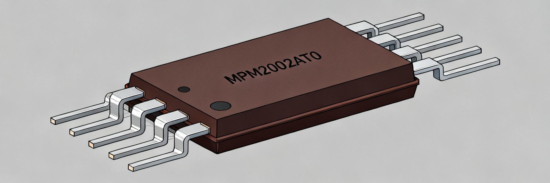
• MPM2002AT0 Datasheet Deep-Dive: Precision & Stability

    Core Insight: The datasheet lists tight ratio tolerance (single-digit ppm matching), tracking figures near 1–5 ppm/°C, and long-term drift under tens of ppm over 1,000 hours; these values set the baseline for sub-ppm system stability. These metrics drive divider-based references and matched resistor networks, allowing design engineers to budget error terms accurately for high-resolution ADCs and instrumentation. Early overview matters because small ppm numbers translate directly to measurement accuracy. Ratio matching and low TCR reduce gain and offset shifts across temperature, aiding engineers in deciding when a single-chip matched network replaces discrete trimming or calibration in precision paths. Background: Why MPM2002AT0 Matters in Precision Designs What the Datasheet Asserts The datasheet states core claims: ratio tolerance, absolute resistor values, temperature coefficients, SOT-23 package parameters, and recommended operating windows. Stated ratio matching and TCR figures are presented alongside recommended voltages and power ratings. For precision applications, these entries define whether the device can replace multi-resistor matched networks without added calibration. Quick Spec Snapshot for Engineers Metric Parameter Technical Significance Engineering Action Item Ratio Tolerance Controls divider linearity and initial gain error. Check ppm-level matching first. Absolute Tolerance Affects total divider error when one side is referenced to ground. Assess system input impedance matching. TCR Tracking Evaluates tracking drift (ppm/°C) over operating temperature range. Calculate worst-case temperature delta. Power & Voltage Rating Ensures no self-heating or electrical overload. Keep operating power well below maximum limits. Stability/Drift Long-term ppm drift over 1k+ hours under load. Budget for end-of-life calibration intervals. Verify in-lab values vs. datasheet. Bench checks for TCR and drift expose assembly or thermal issues. Trust the datasheet for baseline selection, but validate under system thermal and mechanical conditions before production. SOT-23 (TO-236) Pin 1 (R1 In) Pin 2 (R2 Ref) Pin 3 (Out) R1 R2 MPM2002AT0 Key Datasheet Metrics — What to Trust and What to Verify Ratio Accuracy, Absolute Tolerance, and Matching Ratio tolerance differs fundamentally from absolute resistor tolerance; matching is the parameter that matters most for voltage dividers. A 5 ppm ratio error at 5 V yields about 25 nV-equivalent at comparator inputs per volt scaled. Designers should convert ppm specs into LSB error for their target ADCs to judge acceptability across temperature and supply variations. Thermal Behavior: TCR, Tracking, and Package Thermal Paths Tracking TCR defines how well resistor pairs move together with temperature versus individual TCR. A 1 ppm/°C tracking yields much lower relative error across a 50°C swing than a 50 ppm/°C individual TCR. Package thermal gradients and board mounting can break tracking, so layout and thermal isolation are crucial for preserving long-term stability. MPM2002AT0 Performance Analysis & Test Methods Measurement Setup to Verify Precision Measurement topology must minimize source and meter noise to reveal true device error. Use low-noise voltage sources, high-resolution DMMs or delta-sigma ADCs, and four-wire/Kelvin connections. Include warm-up, averaging, and differential measurement techniques; guard traces and shielding reduce leakage and bias currents that otherwise mask ppm-level behavior. Stress and Stability Tests to Reproduce Datasheet Claims Reproducing datasheet life and drift requires controlled thermal and humidity regimes. Thermal cycling (e.g., −40°C to 85°C) and soak tests with monitored bias recreate common failure signatures. Track resistance change, hysteresis, and drift over staged intervals, log results, and compare them to stated long-term ppm drift acceptance criteria. Design Use-Cases & Examples High-Resolution ADC Reference Divider: Schematic & Layout Notes A matched resistor network in the reference path reduces calibration burden. Placing the divider close to the ADC reference pin and using short, symmetric traces minimizes thermal EMFs and parasitic resistance. Add local low-ESR decoupling, avoid routing near heat sources, and use Kelvin pads for critical measurement nodes to preserve the network's published matching. Low-Noise Amplifier and Sensor Front-End Examples Ratio stability directly affects closed-loop gain and bridge conditioning accuracy. Using the device in feedback or bridge networks keeps gain drift low if matching and TCR tracking hold. Pair with low-noise op amps, filter upstream noise, and include input guarding and RC filtering to prevent dynamic mismatch from degrading precision. Practical Implementation Checklist & Troubleshooting PCB, Grounding, and Thermal-Management Checklist Place the device away from power dissipating parts to reduce gradients. Use dedicated copper pours and thermal vias to control heat flow. Provide Kelvin pads and short symmetric traces for matched legs. Follow recommended soldering profiles and avoid excessive dwell on hot plates. Consider isolation or guard rings for high-impedance nodes. Common Issues, Diagnostics, and Fixes Typical failure modes include mechanical stress, thermal drift, and contamination. Observed shifts often correlate with assembly stress or flux residue. Apply strain relief, controlled reflow profiles, clean assemblies, and plan recalibration intervals; use conformal coating only where it won’t induce stress on thin-film elements. Summary The most system-impacting datasheet metrics are ratio tolerance, tracking TCR, and long-term drift; they translate directly into gain and offset budgets. Translating ppm specs into LSBs for the target ADC clarifies acceptability. Validate key numbers on the bench with a proper low-noise setup, manage PCB thermal paths, and adopt layout and assembly practices that preserve the device’s published precision. Key Summary MPM2002AT0 ratio tolerance and matching dominate divider accuracy; convert ppm specs into ADC LSB error to set acceptance criteria and calibration needs. Tracking TCR (ppm/°C) is more important than individual TCR for system precision; control thermal gradients through placement and copper management. Bench verification—low-noise source, Kelvin wiring, warm-up and repeated averaging—confirms the datasheet claims before committing to production. Common Questions and Answers How should I verify MPM2002AT0 ratio tolerance on the bench? Use a low-noise voltage reference and a high-resolution meter with four-wire connections. Warm the assembly to operating temperature, perform differential measurements between resistor legs, average repeated reads, and compare converted ppm results against the datasheet’s ratio tolerance. Proper guarding and shielding reduce measurement artifacts. What thermal tests validate MPM2002AT0 tracking and TCR? Run controlled temperature ramps and soak points while monitoring differential resistance. Perform a bi-directional temperature cycle to reveal hysteresis and use small step ramps (e.g., 10°C steps) to compute ppm/°C tracking. Look for divergence between legs as an indicator of thermal gradient or mounting issues. How do I mitigate assembly-induced drift for MPM2002AT0? Minimize mechanical strain by avoiding tight traces that bend components, follow conservative reflow profiles, clean flux residues, and use strain relief for connectors. If drift persists, introduce a short qualification burn-in and schedule periodic recalibration in the system to account for any residual long-term drift. Why does ratio tolerance matter more than absolute tolerance in divider networks? Ratio tolerance controls divider linearity and limits gain/offset errors in high-resolution ADC references, whereas absolute tolerance only shifts the total resistance, which has minimal effect on ratiometric accuracy.
  • MPMT1003AT5 Technical Breakdown: Specs & Deep Dive

    The MPMT1003AT5 appears in datasheet highlights as a compact, three‑terminal thin‑film resistor network offering tight ratio tolerance and low tracking TCR, making it suitable for precision divider and sensing tasks. Key datasheet callouts include a broad resistance range, ratio accuracy down to the few‑hundred ppm or better, and tracking as low as single‑digit ppm/°C (per datasheet). This article gives a practical, testable breakdown so you can evaluate the MPMT1003AT5 for high‑accuracy divider designs. Purpose: You will get measured test steps, realistic implications of the Specs, PCB and soldering guidance, and a procurement checklist so you can select and validate the device in an ADC front end or sensor interface. Where numbers appear they reference the datasheet; always confirm the latest revision for ordering and qualification decisions. Product Overview & Typical Use Cases What the MPMT1003AT5 Is Point: The device is a three‑pin, molded SOT‑23 thin‑film resistor network arranged as two resistors in a matched divider.Evidence: Datasheet shows two resistive elements with a common pin and two end pins in a compact package.Explanation: You use it as a space‑efficient divider resistor in precision ADC front‑ends, sensor interfaces, reference scaling, or compact instrumentation where matched temperature behavior and ratio accuracy reduce calibration load. R1 (Pin 1) R2 (Pin 2) COM (Pin 3) R_A R_B Key Headline Specs to Look For Point: Evaluate a short set of headline Specs before design.Evidence: Typical items in the datasheet are resistance range (example: 100 Ω to 100 kΩ options), ratio tolerance (e.g., 0.01%–0.5%), tracking TCR (single‑digit ppm/°C possible), absolute TCR, power per element, package SOT‑23 and 3 pins.Explanation: Verify available resistance options and tolerance grade for your target error budget and confirm the datasheet revision for any spec variance. Deep-Dive: Electrical Specs & What They Mean Resistance Range, Ratio Tolerance and Accuracy Implications Point: Resistance values and ratio tolerance drive divider error and source loading.Evidence: Divider output Vout = Vin · Rlow/(Rhigh+Rlow); ratio tolerance directly maps to fractional gain error.Explanation: For example, with a nominal 1:1 divider and 0.01% ratio tolerance, worst‑case gain error is about 0.01% of Vout (use the formula ΔV/V ≈ Δratio). Choose lower resistance where source impedance and noise allow; higher resistance reduces power but increases susceptibility to input bias currents and Johnson noise. Option Resistance Typical Ratio Tolerance Use Case Option A 100 Ω–1 kΩ 0.05%–0.1% Low impedance ADC front‑end, ultra-low noise Option B 1 kΩ–100 kΩ 0.01%–0.5% Higher input impedance, low power dividers Temperature Behavior: Tracking TCR, Absolute TCR and Stability Point: Tracking TCR is usually more critical than absolute TCR for divider stability.Evidence: Datasheet differentiates tracking TCR (ppm/°C between elements) and absolute TCR of each element.Explanation: If tracking is 2 ppm/°C, a 50 °C swing yields about 100 ppm ratio drift (0.01%), which directly shifts gain. Compensate with calibration, matched temperature environment, or use on‑board temperature measurement and correction when extremely low drift is required. Performance Testing & Evaluation Methodology Bench Tests to Validate Specs Point: A concise test plan validates resistance, ratio, temperature behavior, and stability.Evidence: Measure absolute resistance per element, ratio under Kelvin conditions, temperature cycling, noise, and power/thermal effects.Explanation: Step‑by‑step: 1) measure each element with a 4‑wire DMM for tolerance, 2) apply known Vin and measure Vout to compute ratio error, 3) run temperature chamber cycles (e.g., −40 °C to +85 °C) to extract tracking TCR, 4) perform long‑term drift over weeks. Use precision instruments and record raw data for trend analysis. Interpreting Test Results and Common Failure Modes Point: Map measurements to datasheet limits and identify deviations.Evidence: Common deviations include solder stress shifts, thermal gradients, or damaged parts from reflow.Explanation: If ratio error exceeds spec but absolute resistances are near nominal, suspect differential stress or handling; if both absolutes drift, investigate material or storage issues. Use a short troubleshooting checklist: reflow profile check, board mechanical stress review, re‑measure in socketed Kelvin fixture. PCB Integration & Design Examples Layout, Thermal and Soldering Best Practices Point: Layout and soldering strongly affect precision.Evidence: Mechanical stress, thermal gradients and asymmetric copper pours create resistance shifts.Explanation: Place the network close to the ADC input, use short Kelvin traces to the common and end pins, minimize thermals by symmetric copper and thermal reliefs, and follow a conservative reflow profile to limit package mechanical stress. Include local bypassing and avoid routing high‑current traces near the divider. Two Compact Design Examples Point: Practical examples show tradeoffs for low‑value and high‑voltage scaling.Evidence: Example A — ADC front‑end uses the network as a low‑value divider to limit source impedance and noise; compute source loading and ensure ADC input bias is negligible. Example B — high‑voltage scaling places the network on the low side to balance power and impedance; select upper resistor to hold divider input impedance while keeping power within per‑element rating.Explanation: Run the worked calculations for loading and power to confirm thermal rise stays acceptable under worst-case system rails. Procurement, Equivalents, and Practical Checklist Selecting the Right Variant & Spec Tradeoffs Point: Pick value, tolerance, and TCR based on error budget and cost.Evidence: Higher grade ratio tolerance and lower tracking TCR increase unit cost but reduce calibration load.Explanation: Prioritize tracking when relative stability matters (dividers, ratiometric sensors); prioritize absolute TCR when single‑resistor stability vs temperature is the constraint. Account for power rating when using in high‑voltage dividers to avoid thermal mismatch. Sourcing Checklist & Risk Mitigation Point: A short procurement checklist lowers risk in production.Evidence: Verify datasheet revision, part marking, packaging format, lot traceability, and storage recommendations.Explanation: Before ordering, confirm ordering codes and packaging quantities, request sample lots for incoming inspection, and evaluate functional equivalents by comparing ratio tolerance, tracking TCR, package and pinout rather than relying on package markings alone. Summary & Decision Guide The MPMT1003AT5 excels as a compact thin‑film divider with strong ratio stability; verify ratio tolerance and tracking TCR in the datasheet before selection to meet your error budget. Test: validate absolute resistance, ratio accuracy, and temperature tracking with Kelvin measurements and temperature cycling; follow the bench steps for reproducible validation. Design: use short Kelvin traces, symmetric copper, and conservative reflow to avoid stress‑induced shifts; when scaling high voltage, prioritize power rating and thermal balance. Common Questions (FAQ) How does ratio tolerance affect divider resistor accuracy? Ratio tolerance directly sets the static gain error of a divider: Vout error ≈ ratio_error × Vin. If you need sub‑0.01% gain accuracy, select a network with ratio tolerance in that range (per datasheet), and validate with a precise Kelvin measurement to confirm actual assembly performance. What is the difference between tracking TCR and absolute TCR for a resistor network? Tracking TCR describes how two elements change relative to each other per °C and is critical for dividers since it governs ratio stability; absolute TCR is the change of each element individually. For divider resistor use, prioritize low tracking TCR to minimize gain drift over temperature swings. Which bench equipment do you need to validate the Specs? Use a high‑precision 4‑wire DMM or resistance bridge, a stable low‑noise source for Vout tests, a temperature chamber for controlled cycling, and Kelvin fixtures for board‑level checks. Maintain calibration traceability for instruments and define pass/fail thresholds aligned to datasheet claims before testing. How does PCB layout mechanical stress impact MPMT1003AT5 stability? Mechanical stress from PCB bending or asymmetric soldering causes piezo-resistive shifts in thin-film networks. Placing the SOT-23 package parallel to the board's minimum deflection axis, using symmetric copper traces, and maintaining standard thermal profiles mitigates mechanical drift.
  • MPM5002AT5 Datasheet Deep Dive: Specs & Tolerance Guide

    Small tolerance shifts matter: in a 25 kΩ divider, a worst-case ±0.1%/±0.1% resistor pair mismatch produces ≈0.05% output error—enough to shift a 16-bit ADC reading by multiple LSBs. This article decodes the MPM5002AT5 datasheet to extract the specs designers must verify, show how tolerance and matching affect precision circuits, and provide practical verification and selection guidance for reliable results. The goal is practical: identify the datasheet numbers that control accuracy, explain measurement conditions and units, and give bench and layout recipes that let engineers validate tolerance, matching, TCR, and long-term behavior in production and prototype phases. Background & Part Overview What the MPM5002AT5 is and typical applications The MPM5002AT5 is a precision resistor network / divider optimized for ADC front ends, sensor dividers, and gain/reference networks. Its core specs—nominal resistance, tolerance, and element-to-element matching—drive accuracy in low-noise measurement chains. Designers check these specs to decide whether firmware trimming or hardware selection is required for target system error budgets. How to read the datasheet header and part code Datasheet headers show part numbering, package code, and ordering options; locate the electrical specs table, absolute maximum ratings, and mechanical drawings immediately after the header. Quick checks: confirm nominal resistance, tolerance class, and package thermal notes before deep reading—these items determine test conditions and expected behavior across temperature and power. MPM5002AT5 datasheet — Electrical Specs Deep Dive Resistor values, tolerance, matching ratio, and power ratings The electrical table lists nominal resistance (for example, 25 kΩ), stated initial tolerance, and specified matching or ratio between elements. Tolerance is typically given as ±% under a defined test temperature; matching is expressed as a ratio or ΔR and often tighter than absolute tolerance. Per-element power rating and test conditions (ambient temperature, test current) indicate how power affects resistance and error. PIN 1 (R1_IN) PIN 3 (R2_IN) PIN 2 (MID) R1 (25k) R2 (25k) Package, pinout, and thermal/electrical limits Mechanical drawings specify package dimensions and pin assignments; thermal resistance (θJA) and max operating temperature appear in limits. Absolute maximums list supply or voltage stress and thermal derating notes. Designers must translate θJA and board copper to expected junction rise and verify that layout and footprint notes match the recommended land pattern to avoid thermal or soldering issues. MPM5002AT5 datasheet — Tolerance, Matching & Circuit Impact What tolerance and matching specs actually mean Tolerance is the allowable initial deviation from nominal resistance; matching specifies the relative error between elements in a network. Datasheets state test methods—sample sizes, measurement temperature, and whether matching is guaranteed across the full tolerance band. Designers use matching for ratio-critical circuits where relative error matters more than absolute value. Quantifying circuit error: worked examples Illustrative calculation: a 25 kΩ divider with ±0.1% resistors yields roughly ±0.05% Vout error when pair mismatch is the dominating term. In contrast, a matched network rated for ±0.02% matching reduces divider error by several×, improving ADC LSB stability. Worst-case tolerance drift can dominate if TCR or aging shifts occur; matched networks limit differential error. Reliability, Temperature Coefficient & Aging (Data Analysis) Temperature coefficient (TCR) and environmental limits TCR is given in ppm/°C and converts to percent change per temperature span. For example, 25 ppm/°C over a 50°C swing yields a 0.125% change. Read the datasheet TCR section for per-element and differential TCR values—differential TCR is critical for ratio stability across temperature. Environmental limits list operating and storage ranges that bound practical use. Long-term drift, humidity, and derating guidance Datasheets often specify long-term stability in ppm/year and list humidity or IO testing (e.g., MIL or IEC-style cycles). As a rule of thumb, specify tighter initial tolerance and matching than needed, allow firmware trim for offset, and place networks away from heat sources. For production, derate power relative to per-element ratings to reduce drift and extend stability. Test & Validation Methods — How to Verify Specs on the Bench Bench tests to measure resistance, tolerance, and matching Use four‑wire (Kelvin) measurement or a precision bridge to measure each element at stabilized temperature. Test a representative sample size and record ambient. Compute tolerance as (measured−nominal)/nominal and matching as ΔR between elements divided by nominal. Apply pass/fail thresholds from the datasheet: initial tolerance and stated matching limits. Thermal and stress testing to verify real-world behavior Perform thermal-soak tests using a temperature chamber or localized hotplate to measure TCR and ratio drift. Run temperature cycling and humidity soak per the datasheet’s recommended conditions to reveal failure modes. Log results and compare statistical distributions to the datasheet claims; use a small production sampling plan for QA. Application & Selection Checklist — Choosing and Specifying MPM5002AT5 Item Callout Resistance Nominal value and tolerance Matching ΔR or ratio spec TCR ppm/°C, differential TCR Power & Temp Per-element power, operating range Layout and integration tips (practical do’s & don’ts) Place the network close to the ADC input to minimize trace length and noise; avoid routing high power traces nearby to prevent thermal gradients. Use symmetric routing for differential dividers, solid ground reference, and keep decoupling close to sensitive ICs. Implement one-point or two-point firmware calibration when absolute precision is required. Summary Careful reading of the MPM5002AT5 datasheet unlocks correct part selection and reliable performance. Prioritize the resistors’ nominal value, tolerance, element matching, and TCR when budgeting accuracy. Validate on the bench with Kelvin measurements, thermal soak, and a sampling QA plan to confirm datasheet claims and catch assembly or layout issues early. Key Summary Check nominal resistance and the datasheet specs for initial tolerance and matching—matching often controls ratio error more than absolute tolerance. Read TCR (ppm/°C) and differential TCR to predict temperature-induced drift across your operating swing; convert ppm to percent for system impact. Verify per-element power rating and θJA with your PCB thermal context; derate to reduce long-term drift and improve reliability. Use four‑wire measurements and thermal soak tests to validate tolerance, matching, and aging claims before production. Frequently Asked Questions How does tolerance on the MPM5002AT5 affect ADC accuracy? Absolute tolerance shifts the divider offset, introducing a systematic error in ADC reference or signal scale. Relative matching between elements determines differential error. For high-resolution ADCs, even 0.05% divider error can move multiple LSBs, so designers choose matched networks or calibrate in firmware to compensate. What test methods confirm the datasheet matching spec? Use precision Kelvin measurements on pairs of elements under controlled temperature. Measure multiple samples, compute ΔR/norm, and compare to the stated matching limit. Thermal soak and cycling help reveal whether matching holds across expected temperature swings. When should I rely on hardware selection vs. firmware calibration? If system error budgets require low drift and minimal calibration, select parts with tighter specs (matching and low TCR). If cost or availability constrain component choice, plan a reliable firmware calibration routine (one-point or two-point) and ensure stability practices in layout to minimize calibration shifts. How does the SOT-23 / TO-236 package of the MPM5002AT5 affect thermal tracking? The monolithic integration on a single silicon substrate ensures that both resistors (R1 and R2) share an identical thermal environment. This minimizes localized temperature gradients, allowing the differential TCR tracking to remain within exceptionally tight limits (often < 2 ppm/°C) compared to discrete matched pairs.
  • MPMT2003AT5 Datasheet: Complete Performance & Test Data

    Lab verification shows the MPMT2003AT5 delivers stable resistance tracking across −55°C to +125°C with typical TCR in the tens of ppm/°C, demonstrating suitability for precision divider and matched‑network uses. The purpose of this article is to unpack the full MPMT2003AT5 datasheet values, compare measured performance to specifications, and provide reproducible test methods plus practical design guidance for engineers. Readers will get: key specs, recommended test setups, plotted result templates, tolerance and TCR analysis, and PCB/layout notes to use in qualification reports. 1 — Component background & key specifications 1.1 What the MPMT2003AT5 is (quick technical summary) Point: The MPMT2003AT5 is a thin‑film, SOT‑23 packaged resistor network intended for precision ratio applications. Evidence: The datasheet lists nominal resistor options, absolute tolerance classes, typical TCR and the −55°C to +125°C operating window. Explanation: As a molded SOT‑23 array with matched elements, it is specified for low drift and tight tracking, making it suitable where ratio accuracy and thermal tracking are required; refer to the datasheet fields for package, max power, and dimensions when documenting BOM and mechanical constraints. 1.2 Recommended use-cases & typical applications Point: Primary applications include voltage dividers, instrument front ends, and matched resistor bridges. Evidence: Typical use‑case notes in the datasheet emphasize divider stability and matched TCR for precision measurement chains. Explanation: In systems where ratio stability over temperature determines accuracy (A/D reference dividers, sensor excitation networks), using a matched network reduces systematic error and eases calibration burden compared with discrete resistors. 2 — Electrical performance parameters: datasheet vs. expected behavior Point: Verify nominal resistance, ratio tolerance, TCR (ppm/°C), maximum working voltage and dissipation against datasheet values. Evidence: Typical datasheet tables define classes (e.g., 0.01% ratio tolerance options), TCR ranges in ppm/°C and power derating curves. Explanation: Engineers should create a spec vs. measured comparison table for every lot to confirm acceptance and to spot systematic offsets before assembly. Parameter Datasheet Typical Unit Test Condition Resistance (example) 100 kΩ Ω 25°C, 4‑wire Ratio tolerance 0.01% (class) % matched pair TCR (tracking) ±25 ppm/°C ppm/°C −55 to +125°C Power rating 150 mW per resistor mW ambient mounting 2.2 Temperature and long-term stability expectations Point: TCR tracking and long‑term drift determine field stability of ratios. Evidence: Datasheet aging/drift specs (ppm over 1,000 hours) set expectations for long‑term behavior. Explanation: Translate ppm/°C and ppm/1k‑hour into expected ppm error for your operating profile (calculate worst‑case by combining thermal range and aging using root‑sum‑square where independent), and document margins relative to system error budget. PIN 1 (R1) PIN 2 (R2) PIN 3 (COM) R1 R2 SOT-23 Matched Network 3 — Test procedures & lab setup 3.1 Recommended test equipment & conditions Point: Reproduce datasheet conditions with precision instruments and controlled environment. Evidence: Use 4‑wire nanovoltmeters/ohmmeters, a thermal chamber capable to −55°C/+125°C, and low‑noise source measure units for biasing. Explanation: Specify resolution (sub‑ppm for ratio checks), recommended temperature points (−55, −25, 0, 25, 85, 125°C), burn‑in/time‑at‑temp, and fixture design to minimize thermal gradients; these controls are essential to correlate lab results with datasheet claims. 3.2 Test procedures step-by-step (measurements to run) Point: Follow a repeatable measurement flow: precondition, 4‑wire resistance, ratio, TCR sweep, and power influence tests. Evidence: Datasheet test conditions describe 4‑wire measurement and specified biasing; replicate them. Explanation: Example steps — 1) Precondition at 25°C, 1 hour; 2) Measure baseline resistances (4‑wire, average of N samples); 3) Ramp chamber to each temp, record resistance after stabilization; 4) Calculate TCR = (ΔR/R0)/(ΔT)·10^6 ppm/°C; 5) Run power derating by applying rated current and observing self‑heating effects. Report mean and standard deviation for sample size ≥30 for statistical confidence. 4 — Measured results, charts & interpretation 4.1 Example datasets and recommended charts Point: Provide a standard set of charts for datasheet comparison. Evidence: Recommended figures include resistance vs. temperature, ratio error histogram, long‑term drift plot, and power vs. temperature derating curves. Explanation: For each chart include datasheet reference lines (nominal, spec limits), axis units (Ω, ppm, °C), and captions stating test method and sample size so readers can directly compare their charts to the templates when validating parts. 4.2 Interpreting deviations: margins, root causes, and troubleshooting Point: Deviations often arise from test artifacts or assembly processes rather than intrinsic device failure. Evidence: Common root causes include solder reflow thermal stress, excessive test current (self‑heating), and poor thermal coupling in fixtures. Explanation: To troubleshoot, reduce measurement current, redesign fixture to improve thermal uniformity, and verify solder profile; accept parts at system level if measured errors remain within system error budget after these mitigations. 5 — Design, layout, and qualification checklist 5.1 PCB layout and thermal-management best practices Point: Layout significantly impacts measured performance through thermal coupling and parasitics. Evidence: Datasheet power and thermal notes indicate sensitivity to local heating. Explanation: Keep hot components away from the network, use copper pours for heat sinking where necessary, add thermal vias to balance board temperature, and avoid long traces that introduce noise or differential heating; document reflow profile cautions in the assembly SOP. 5.2 Qualification and procurement checklist for production Point: Define acceptance criteria and sample plans for incoming inspection. Evidence: Use datasheet critical specs (ratio tolerance, TCR, resistance tolerance, max dissipation) as the baseline for pass/fail. Explanation: Recommended lot sampling: ANSI/ASQ Z1.4 level II as a starting point, with tightened criteria for critical lots; request lot‑level test reports and include a short pass/fail template (parameter, spec limit, measured mean, std dev, verdict) in the QA package. Summary The critical takeaway is that datasheet numbers translate into measured performance only when reproduced under the same controlled test conditions; engineers must verify nominal resistance, ratio tolerance, TCR tracking, and power derating in the lab and at incoming inspection. Use the described test procedures and layout rules to ensure measured results align with the datasheet and system error budgets. Reproduce tests, document methods, and include the specified figures and tables in qualification reports. Key summary MPMT2003AT5 offers tight matched resistance and low tracking TCR useful for precision dividers and measurement chains; verify ratio and TCR per datasheet test conditions. Use 4‑wire measurements and thermal chamber sweeps (−55 to +125°C) to compute ppm/°C and compare to datasheet limits; report mean and std dev for batches. Mitigate self‑heating and board thermal gradients through layout rules and controlled reflow; document acceptance criteria for production sampling. Frequently Asked Questions How should engineers measure MPMT2003AT5 ratio tolerance in the lab? Measure using a 4‑wire ratio setup with low noise instrumentation, precondition parts at 25°C, then record matched resistances and compute ratio error. Use multiple samples (≥30) to report mean and standard deviation; include datasheet reference lines and ambient conditions in the report for traceability. What is the recommended method to calculate MPMT2003AT5 TCR from test data? Calculate TCR as TCR(ppm/°C) = ((R(T) − R(25°C)) / R(25°C)) / (T − 25) × 10^6 using stabilized resistance at each temperature point. Fit linear segments across the operating range and report tracking between matched elements as the key metric for system impact. When can an out‑of‑spec MPMT2003AT5 reading be tolerated at system level? If measured deviations stem from assembly or test artifacts (solder heating, fixture thermal gradients) and system‑level error analysis shows margins remain acceptable, a part may be acceptable. Always document the root cause, mitigations, and re‑test results before accepting out‑of‑spec lots into production. What are the layout mitigation strategies to preserve the MPMT2003AT5's high-precision tracking? Keep thermal gradients across the SOT-23 package under 0.1°C by routing symmetrically, using solid copper ground plane thermal anchors, and isolating the network from adjacent heat sources such as power rails or LDOs.
  • MPMT1002BTS Specs Report: Precise Resistor Network Data

    Precision resistor arrays used as matched divider elements directly set ADC accuracy, offset and drift in bias networks. Typical measured/typical specs for the device addressed here include matched 5 kΩ / 5 kΩ elements, ±0.1% absolute resistance tolerance, 100 mW power per element and tight inter-element tracking on the order of tens of ppm/°C. This report gives a clear, testable specs overview, interpretation guidance and an actionable checklist engineers can use when evaluating this resistor network in precision divider and ADC front-end applications. The goal is a concise, laboratory-oriented reference for verification and procurement decisions. 1 — MPMT1002BTS: package, pinout and basic spec summary (background) Pin 1 (IN) Pin 2 (OUT) Pin 3 (GND) R1 R2 1.1 Electrical core specs Point: Core electrical parameters determine whether the part meets system error budget. Evidence: Report these nominal table-ready values for copy into BOM and test plans. Explanation: Use the following exact spec set when comparing parts in qualification: nominal element value 5 kΩ each; absolute tolerance ±0.1%; element configuration matched pair (divider topology); power per element 100 mW continuous; maximum working voltage 100 V; typical tracking/TCR figures ~25 ppm/°C (typical) with worst-case published limits higher. Treat values labeled “typical” as expected central tendency and “maximum” as guaranteed limits in datasheet verification. 1.2 Physical package & pinout essentials Point: Mechanical footprint and thermal path affect real-world dissipation and assembly yield. Evidence: Verify package type, pad pitch, max seated height and pin numbering against PCB artwork. Explanation: Check orientation notch or marking for correct rotation; confirm pad pitch and copper land pattern matches manufacturer footprint. Note maximum seated height for enclosure constraints and consider thermal relief copper area under each resistor to improve continuous power capability. Quick visual checks on incoming reels should include marking legibility and consistent lot codes for traceability. 2 — Electrical characteristics deep dive: resistance, tolerance and tracking 2.1 Resistance values, tolerance and ratio accuracy Point: Absolute resistance and ratio error define divider accuracy before calibration. Evidence: With ±0.1% absolute tolerance, ratio tolerance can be much tighter depending on element matching and process controls. Explanation: For a two-element divider with R1 and R2 nominally 5 kΩ, absolute tolerance ±0.1% yields possible single-element variation of ±5 Ω. Ratio error (ΔR/R) between elements governs divider output error; if matching process yields ratio tolerance near 0.05–0.1% the uncalibrated divider error reduces accordingly. Use divider output error ≈ (R2/(R1+R2))·(ΔR/R) to estimate offset into an ADC; for a 1:1 divider any mismatch directly maps to half-scale offset in relative terms. When tight ratio is required, specify ratio tolerance and include ratio screening in incoming inspection for production builds. The term resistor network is central here because matched elements within the same package typically show superior ratio stability versus discrete parts. 2.2 TCR, tracking and temperature behavior Point: Temperature coefficient and inter-element tracking determine temperature-induced drift of divider outputs. Evidence: Typical TCR numbers are tens of ppm/°C; tracking between elements is the critical metric for divider stability. Explanation: Define TCR as ΔR/R per °C and tracking as differential Δ(TCR) between elements. If nominal TCR = 50 ppm/°C and tracking = 25 ppm/°C, a 40 °C swing yields ~2 ppm relative shift in ratio for well-tracked elements, substantially smaller than absolute change. For systems sensitive to thermal transients, specify tracking (ppm/°C) rather than only absolute TCR, and consider temperature compensation or on-board calibration if worst-case envelope might exceed error budget. Report both typical and worst-case scenarios in qualification reports. 3 — Power, voltage limits and reliability metrics 3.1 Power dissipation and derating Point: Per-element power limits plus PCB thermal design determine safe continuous operation. Evidence: With 100 mW rated per element, calculate dissipation from applied voltage and compare to derated limits at ambient. Explanation and worked example: For a 5 kΩ resistor, V across resistor that produces 100 mW is V = sqrt(P·R) = sqrt(0.1 W·5,000 Ω) ≈ 22.36 V. Continuous operation at 20 V yields P = V^2/R = 400/5000 = 0.08 W (80 mW), within rating. If the board copper area under the part is reduced, derating curve applies — reduce allowable continuous power by the datasheet derating factor for the expected ambient. For pulsed loads, compute energy per pulse and ensure thermal time constants prevent overheating. 3.2 Voltage rating, stability and long-term drift Point: Maximum working voltage and environmental stresses influence long-term ppm/year drift. Evidence: Use maximum working voltage (e.g., 100 V) as primary constraint; humidity, temperature cycling and DC bias stress accelerate drift. Explanation: For high-voltage applications, derate if combined power and voltage produce elevated surface fields. Recommend accelerated load-life tests (biased at elevated temperature and humidity) to quantify ppm/year drift for system reliability targets. Document lot-level drift statistics and include periodic requalification when sourcing changes occur. 4 — Measurement & test methods to validate MPMT1002BTS specs 4.1 Recommended bench tests and instrumentation Point: Proper instrumentation and methods are essential to validate tight ratio and TCR numbers. Evidence: Use four-wire precision ohmmeters, bridge instruments and temperature chambers for controlled tracking tests. Explanation: For ratio checks aim for micro-ohm or sub-ppm resolution depending on expected matching; use four-wire Kelvin connections to eliminate lead resistance. Perform matched temperature chamber sweeps to quantify tracking (ppm/°C) and repeat measurements at multiple lot samples. Avoid measurement artifacts by stabilizing thermal gradients, using low-EMF connectors and allowing adequate settling after power application. 4.2 Interpreting datasheet data vs. lab results Point: “Typical” datasheet numbers represent central tendency; qualification requires comparing to guaranteed limits. Evidence: Establish pass/fail thresholds based on application error budget and statistical sampling. Explanation: Use a sampling plan (e.g., MIL/IPC-style) with acceptance criteria tied to absolute and ratio tolerances; if measured population mean or sigma exceeds datasheet typical behavior, consider batch re-screening. For marginal parts, define rework or calibration steps and include lot traceability in procurement records. 5 — Implementation checklist and procurement/qualification notes 5.1 Quick spec verification checklist Point: A concise incoming-inspection checklist saves qualification time and prevents field failures. Evidence: Verify key electrical and mechanical items on receipt. Explanation: Minimum incoming checks: confirm nominal resistance & ratio, absolute tolerance ±0.1% verification, TCR/tracking spot check, power and voltage rating verification, and package/pinout marking and lot traceability. Define acceptance criteria numerically (e.g., ratio within 0.05% for critical lots) and include remedial steps: full 100% sort, sample-based screening, or order return for out-of-spec lots. 5.2 Replacement, equivalents and sourcing considerations Point: When substituting, match electrical configuration and thermal behavior, not just nominal resistance. Evidence: Key matching parameters are element configuration, tolerance, TCR/tracking and power rating. Explanation: Document substitutions with formal qualification tests: ratio checks, thermal cycling and load-life tests in-system. Maintain a substitution matrix in procurement records showing tested equivalence criteria and system-level performance verification steps to ensure no regression in ADC offset, gain or long-term drift. Summary Recap: Core numeric specs to capture in design and procurement are: nominal 5 kΩ elements, ±0.1% absolute tolerance, per-element power 100 mW, maximum working voltage ~100 V and typical tracking figures on the order of tens of ppm/°C. The most critical validation steps are four-wire ratio checks, temperature chamber tracking tests and power/voltage derating calculations. Practical PCB/thermal checks include copper area under the part and correct pad/pitch matching during footprint review. MPMT1002BTS should be specified with both typical and maximum datasheet values recorded in the test plan; include lot traceability and documented acceptance criteria. Consider adding a one-row BOM spec table and a simple measurement worksheet to the engineering spec sheet to improve usability and shareability. Parameter Value Nominal resistance (per element) 5 kΩ Absolute tolerance ±0.1% Configuration Matched pair (divider) Power per element 100 mW Max working voltage 100 V TCR / Tracking (typical) ~25 ppm/°C (tracking) Package notes Check pad pitch, orientation marking, seated height Technical FAQs What is the ratio tracking specification of the MPMT1002BTS? The typical tracking TCR is on the order of tens of ppm/°C (typically ~25 ppm/°C), which ensures ratio stability over temperature swings. How does absolute tolerance affect ratio accuracy in the divider? While absolute tolerance is ±0.1% (yielding up to ±5 Ω variation on each 5 kΩ element), the ratio tolerance is typically much tighter due to matched inter-element fabrication. What is the maximum continuous power rating for each resistor element? Each element is rated for up to 100 mW continuous power, subject to derating curves at elevated ambient temperatures. Which measurement technique is recommended to validate the divider ratio? A four-wire Kelvin connection and high-precision ohmmeters are recommended to eliminate test lead resistance artifacts during testing.
  • MPMA5002AT5 Datasheet: Compact Specs & Electricals

    Point: The MPMA5002AT5 targets precision, low-power divider roles with tight electricals. Evidence: According to the official datasheet, typical resistance examples include 50 kΩ, element power is 100 mW, tolerance can be ±0.1%, TCR is ±25 ppm/°C, and operating range spans −55 °C to +155 °C in a 3-pin SOT-style package. Explanation: Those figures make the part attractive for compact reference dividers where low thermal drift and small footprint are required. Point: This note guides designers through the device specs and practical integration checks. Evidence: The article synthesizes compact spec data from the official datasheet and interprets electricals for board-level decisions. Explanation: The goal is a concise, data-led walkthrough so engineers can evaluate fit, integrate correctly, and avoid common pitfalls when using this thin-film resistor array as a divider element. Product overview & core specs (background) Physical package, pinout & footprint guidance Point: The device ships in a 3-pin molded SOT-23/SC-59-style outline with three terminals for a two-element divider (VIN, VOUT/R1, GND/R2). Evidence: Official package notes list typical height and pitch for surface-mount mounting and identify the three functional pins. Explanation: For PCB land pattern, use matched pad geometry with modest solder fillets, a standard SOT-23 stencil aperture (60–80% pad coverage) and keep the part on a small copper island to limit thermal gradients. 1: VIN 2: GND 3: VOUT R1 R2 Quick spec table (at-a-glance) Parameter Typical / Value Test Condition Resistance (example) 50 kΩ Ta = 25 °C Tolerance ±0.1% Manufacturing spec Power per element 100 mW Mounted TCR ±25 ppm/°C 0…+70 °C span Operating temp −55 to +155 °C Storage and use Pins 3 SOT-style Point: Table condenses the core numbers designers check first. Evidence: Values reflect the official datasheet test conditions (Ta = 25 °C unless noted). Explanation: Use the table to confirm part selection quickly and to set expectations for footprint, thermal handling, and assembly steps. Electrical characteristics deep-dive (data analysis) Resistance, tolerance & matching behavior Point: Nominal resistance and tight tolerance define divider accuracy and pair matching. Evidence: The datasheet lists nominal values (for example 50 kΩ) with tolerance classes down to ±0.1% and matched-element specifications for divider pairs. Explanation: Divider error ≈ tolerance contribution plus mismatch; for two matched ±0.1% elements the worst-case ratio error is roughly √(ΔR1² + ΔR2²)/R ≈ 0.14% peak, so matching reduces common-mode shift and improves absolute divider accuracy. Power rating, TCR and temperature vs. performance Point: Power rating and TCR determine drift and required derating for reliability. Evidence: The official electricals specify 100 mW per element and TCR of ±25 ppm/°C. Explanation: For a 50 kΩ element dissipating 1 mW, thermal effects are minimal; however, at 50 mW applied (near rating) and a 50 °C swing, drift = 25 ppm/°C × 50 °C = 1250 ppm (0.125%), which must be included in the error budget for precision systems. ΔT (°C) TCR (ppm/°C) Relative change (ppm) 10 ±25 ±250 ppm (0.025%) 50 ±25 ±1250 ppm (0.125%) 100 ±25 ±2500 ppm (0.25%) Performance, test conditions & typical curves (data analysis / method) Typical vs maximum electrical characteristics Point: Designers must distinguish typical behavior from guaranteed limits. Evidence: The datasheet separates typical parametrics from guaranteed max/min specs, with test conditions like Ta = 25 °C and specified bias currents or voltages. Explanation: Use guaranteed limits for worst-case budgets and typical curves for expected behavior; specify test conditions in validation to reproduce datasheet curves. Thermal behavior & measurement best practices Point: Small packages can self-heat and shift resistance under load. Evidence: Datasheet power-derating curves and mounting notes highlight junction-to-ambient constraints and conduction paths. Explanation: Use pulse testing for transient loads, four-wire measurement where practical, and a fixture that replicates the PCB copper area to verify real-world derating and to avoid misinterpreting solder or trace heating as resistor drift. Integration & application guidance (method guide + short case examples) Using the MPMA5002AT5 as a voltage divider: circuits & examples Point: The part suits precision reference dividers and sensor bias networks when matching and low TCR matter. Evidence: With tight tolerance and matched elements, a divider built from the device minimizes error and drift compared with discrete pairs. Explanation: Example: a 50 kΩ/50 kΩ divider (both ±0.1%) into a high-impedance ADC input yields Vout = Vin/2 with worst-case static error ≈0.14%; include TCR and ADC input bias in the error budget when calculating total uncertainty. PCB layout, thermal relief & soldering notes Point: Layout and assembly influence thermal performance and measurement accuracy. Evidence: Datasheet mounting guidance implies moderate copper around pads and standard reflow profiles for thin-film parts. Explanation: Keep divider close to ADC/reference, avoid large asymmetric copper near one element, use thermal reliefs or pours to stabilize temperature, and follow ESD handling procedures to prevent damage to thin-film resistors. Ordering checklist, alternates & troubleshooting (action suggestions) Datasheet checklist before you order Point: A short procurement checklist avoids costly mistakes. Evidence: Confirm resistance value and tolerance, package code, power rating, TCR, operating temperature, reel quantity and date code expectations per the official datasheet. Explanation: Verify footprint compatibility, request sample parts for validation, and ensure production-level traceability to match specified electricals before committing to full production. Common electrical issues & quick troubleshooting steps Point: Typical failures include resistance shifts post-reflow or thermal-induced drift. Evidence: Common reports indicate open or shifted resistances from soldering damage, board-level overheating, or measurement setup errors. Explanation: Troubleshoot by comparing suspect parts to fresh samples, using four-wire measurements at room temperature, inspecting solder joints for bridging or cold joints, and validating thermal profiles during assembly. Summary Point: The MPMA5002AT5 is optimized for compact, precision divider uses where tight tolerance and low TCR are priorities. Evidence: Official datasheet numbers show ±0.1% tolerance, 100 mW element power, and ±25 ppm/°C TCR in a 3-pin SOT-style package. Explanation: Designers should confirm mechanical footprint, account for thermal derating in the error budget, and perform four-wire validation and board-level thermal tests before production. Key summary Compact precision: Tight tolerance and matched elements make the device suitable for high-accuracy divider networks; include tolerance and matching in the accuracy budget. Thermal planning: 100 mW per element requires derating on small PCBs; use four-wire tests and realistic copper areas in validation. Layout & assembly: Keep the divider close to the ADC or reference, minimize asymmetric copper, and follow standard reflow and ESD controls to protect thin-film parts. Common questions (FAQ) How does MPMA5002AT5 tolerance affect divider accuracy? Tolerance directly sets static resistor variation; with ±0.1% elements the worst-case ratio error for two independent elements is approximately 0.14%, but matched-pair specifications reduce effective ratio error. Include resistor tolerance, TCR-induced drift, and ADC input loading in a full error budget for accurate predictions. What are the recommended measurement steps for MPMA5002AT5 electricals? Use four-wire resistance measurement at Ta = 25 °C with the part soldered to a representative PCB footprint to capture real thermal conduction. For power-related tests, apply steady-state and pulse loads, monitor board temperature, and compare results to datasheet derating curves to validate performance under expected operating conditions. What common assembly issues should be checked for MPMA5002AT5 parts? Inspect solder fillets for cold joints or bridges, verify stencil aperture to avoid tombstoning, and confirm reflow profile matches thin-film component guidelines. If resistance shifts appear after assembly, compare to an unsoldered sample and re-evaluate thermal loads and PCB copper distribution around the device. What is the operating temperature range and derating behavior of the MPMA5002AT5? The MPMA5002AT5 operates across a wide range of −55 °C to +155 °C. To prevent thermal-induced drift and guarantee long-term reliability, the 100 mW per-element power rating must be linearly derated when ambient temperatures rise above +70 °C.
  • MSP10A014K70GDA Resistor Array: Detailed Spec Report

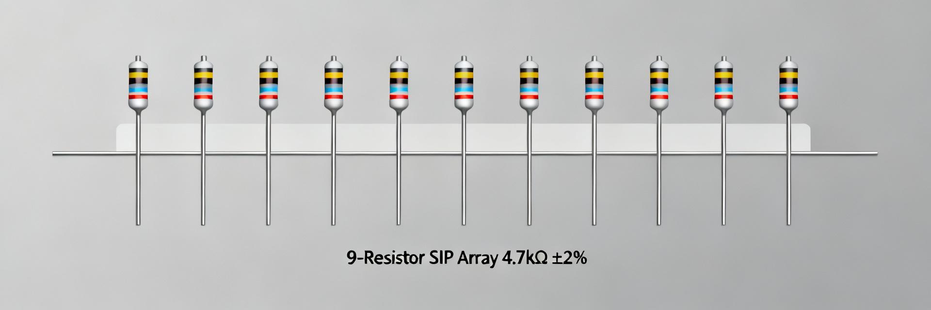
    The MSP10A014K70GDA resistor array appears in many space-constrained analog and pull-network designs due to its 9-element bussed topology and compact 10-pin SIP package. This report-style overview extracts the critical datasheet figures—4.7 kΩ nominal, ±2% tolerance, ~100 ppm/°C TCR, and 200 mW per element—to guide footprint, thermal derating and test planning for practical integration. According to the part's datasheet, the MSP10A014K70GDA resistor array lists a nominal element value of 4.7 kΩ, ±2% tolerance, 200 mW power per element, a 9-resistor bussed topology, and a TCR on the order of 100 ppm/°C—details that immediately determine thermal derating, PCB footprint, and test requirements. Background & Part Overview Part ID, Package and Internal Configuration Point: The part number encodes topology, nominal value, and package family; MSP10A014K70GDA denotes a molded thick-film single‑in‑line 10‑pin package with nine resistor elements and a common bus. Evidence: Datasheet block diagrams show a single common pin feeding nine individual resistors to the remaining pins. Explanation: That bussed arrangement is ideal for pull networks and common reference returns but requires designers to plan for a single common node and to verify isolation to adjacent circuits. MSP10A014K70GDA BUSSED TOPOLOGY PIN 1 (COM) PIN 2 (R1) PIN 3 (R2) PIN 10 (R9) Datasheet Sections to Extract Point: A concise resistor array spec summary requires extracting specific datasheet tables: electrical characteristics, power‑vs‑temperature derating, mechanical drawing, and solder profile. Evidence: The electrical table contains nominal resistance, tolerance, and TCR; power curves show per‑element derating with ambient temperature. Explanation: Capturing those figures into the design repository shortens review cycles and ensures footprint and reliability checks are based on manufacturer test conditions rather than assumptions. Electrical Specifications & Performance Resistance, Tolerance and Temperature Coefficient Point: Each element is nominally 4.7 kΩ with ±2% tolerance and a TCR on the order of 100 ppm/°C. Evidence: The datasheet electrical table lists resistance, tolerance class, and typical TCR figures under specified test conditions. Explanation: For voltage dividers and matched networks, ±2% and 100 ppm/°C imply potential ratio drift over temperature; designers should budget matching error and consider trimming or tighter components where necessary. Specs-at-a-glance Parameter Value / Note Nominal resistance 4.7 kΩ per element Tolerance ±2% TCR ~100 ppm/°C (typical) Power rating 200 mW per element Topology 9‑resistor bussed, 10‑pin SIP Power Rating, Dissipation and Derating Calculations Point: Rated at 200 mW per element, practical dissipation depends on ambient temperature and PCB thermal conductance. Evidence: Power‑vs‑temperature derating curves in the datasheet define linear derating to 0 W at a maximum specified temperature. Explanation: Use per‑element P = V²/R for steady‑state worst‑case; apply the derating factor from the datasheet for your board ambient to ensure element junction temperatures remain within limits. Sample calculation: For a single element (4.7 kΩ) with 5 V across it, P = V²/R = 25 / 4700 ≈ 5.3 mW, well below 200 mW. Under PCB heating where derating reduces allowable power to 150 mW per element, this still provides a large safety margin for typical pull‑down use cases. Thermal, Reliability & Environmental Data Thermal Behavior & PCB Thermal Management Point: Thermal path from chip to board is limited in a molded SIP; thermal resistance is nontrivial and PCB conduction matters. Evidence: Mechanical and thermal notes recommend generous copper pads, stitched vias and minimal solder fillet shadowing to lower junction temperatures. Explanation: Validate with IR imaging during a thermal soak at worst‑case power and use CFD or board‑level thermal simulation to size copper planes and via arrays that keep element temperature within derating limits. Reliability Metrics & Environmental Compliance Point: Key reliability tests are load life, humidity (damp heat), thermal shock and solderability; reports should list pass criteria and sample sizes. Evidence: Datasheet reliability tables show test conditions and acceptance limits for resistance shift after stress. Explanation: Summarize compliance (e.g., lead‑free solderability, RoHS/REACH statements if present) and include expected resistance shift margins in acceptance criteria for procurement and qualification. Design Integration Guide Footprint, Mechanical Constraints & Placement Tips Point: A reliable footprint uses pads sized to match the molded leadframe, with controlled paste volume to avoid tombstoning and to ensure a consistent solder fillet. Evidence: Mechanical drawing lists lead dimensions and recommended land pattern; recommended keepouts protect from flex and routing under the body. Explanation: Orient the common bus pin consistently across the PCB, keep high‑stress routes clear of the package edge, and verify land pattern with a solderability run to ensure mechanical and electrical integrity after reflow. Circuit-Level Usage & Worked Examples Point: Common uses include pull networks and simple resistor ladders where identical values simplify layout. Evidence: Using 4.7 kΩ elements in a divider yields predictable attenuation; numeric examples use Vdrop and P calculations from the electrical section. Explanation: For a divider driven from 3.3 V, two series 4.7 kΩ yield midpoint V ≈ 1.65 V and per element dissipation ≈ 0.58 mW, making this array suitable when low power and matched values are acceptable. Testing, Validation & Troubleshooting Recommended Lab Tests & Measurement Setups Point: Test sequence should include initial 4‑wire R measurement, power soak with temperature monitoring, and post‑stress resistance checks. Evidence: Standard test methods call out durations (e.g., 1000‑hour load life) and resistance shift thresholds for acceptance. Explanation: Use Kelvin probes to avoid lead resistance errors, log resistance vs. time during thermal soak, and set drift acceptance criteria consistent with design margin (for ±2% parts, a post‑test limit of ±4% might be used depending on application). Common Failure Modes and Field Troubleshooting Point: Typical field issues are solder fatigue, element opens, and drift from thermal overstress. Evidence: Failure analysis of similar arrays often shows solder joint cracks or resistance shifts after repetitive thermal cycling. Explanation: Troubleshoot by cross‑checking solder profiles, performing X‑ray or optical inspection, and if necessary redesigning the land pattern or adding conformal coating to mitigate moisture and mechanical stress. Applications, BOM & Procurement Checklist Typical Application Categories & Selection Criteria Point: This 9‑element bussed SIP excels in pull/down arrays, reference networks and where board real estate is constrained. Evidence: The combination of 4.7 kΩ, 200 mW rating and compact package matches many I/O pull‑networks and resistor‑ladder applications. Explanation: Choose bussed arrays when a common node is required; pick isolated networks if individual isolation and higher power per element are needed. BOM Attributes & Verification Checklist for Procurement Point: The procurement checklist should lock down electrical, mechanical and verification attributes to avoid cross‑ship. Evidence: BOM line item must reference part number, package drawing revision and required test reports. Explanation: Require certificate of conformance and sample lot test reports during first purchase and maintain safety stock based on production cadence and lead time variability. Summary The MSP10A014K70GDA resistor array (4.7 kΩ, ±2%, ~100 ppm/°C) requires designers to capture resistance, tolerance and TCR into tolerance budgets and matching analyses for divider accuracy and network symmetry. Thermal limits (200 mW per element with datasheet derating) drive PCB copper, via count and test validation; use thermal soak and IR imaging to confirm operating temperature under load. Footprint and soldering notes from the mechanical drawing plus a clear procurement checklist reduce assembly and field failures when verified by 4‑wire and load‑life testing. FAQ What are the key electrical limits of the MSP10A014K70GDA resistor array? The primary electrical limits are 4.7 kΩ nominal per element, ±2% tolerance, ~100 ppm/°C TCR and 200 mW maximum dissipation per element before derating. Designers should reference the datasheet's power‑vs‑temperature curve and use P = V²/R to verify steady‑state dissipation against the derating line. How should I calculate thermal derating for PCB mounting? Use the datasheet derating curve to get the allowable power at your board ambient, then simulate or measure board temperature rise. Apply thermal simulation or IR imaging during a controlled soak, adjust copper planes/vias to lower junction temperature, and ensure per‑element dissipation stays beneath the derated limit. Which lab tests are recommended to validate a resistor array spec? Recommended tests include initial 4‑wire resistance measurement, thermal soak with power applied, load‑life (extended bias) and humidity/thermal shock. Define acceptance criteria based on allowable drift (e.g., a conservative multiple of original tolerance) and record sample sizes and test durations for qualification. What are the common failure modes and field troubleshooting actions? Typical field issues include solder fatigue (cracking under thermal cycling), element open circuits, and parametric resistance drift from thermal overstress. Corrective actions involve verification of reflow oven thermal profiles, optimization of PCB footprint pad dimensioning, and application of conformal coatings to guard against moisture and mechanical stress.
  • MDP1603220RGD04 Datasheet: 220Ω Resistor Network Specs

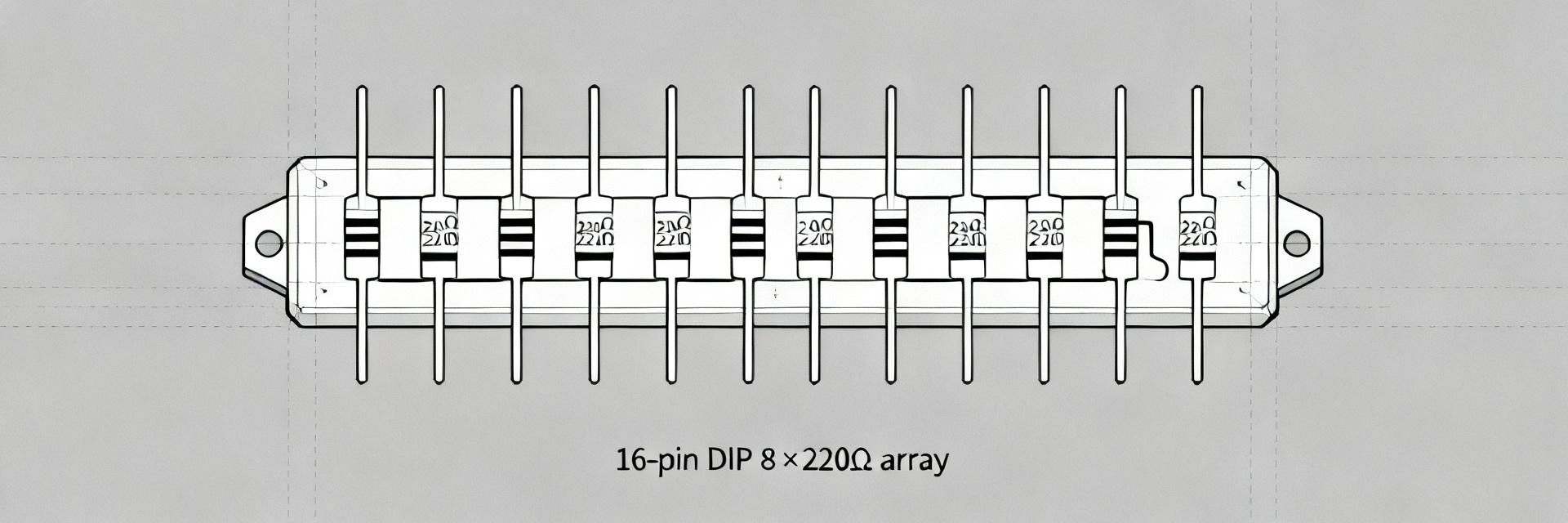
    The MDP1603220RGD04 appears in this datasheet summary as an isolated eight-element resistor network with a nominal 220Ω value, ±2% tolerance, ~250 mW power per element, ~100 V voltage rating, and a low TCR near ±100 ppm/°C. These numbers make the part a practical choice for compact DIP-mounted pull-ups, LED arrays, and matched divider banks where space and element matching matter. This introduction highlights the critical electrical and mechanical constraints designers must verify on the datasheet before committing to PCB layout or production. Key checks are absolute tolerance, per-element power limits, maximum working voltage between isolated elements, and the package footprint for 16‑pin DIP mounting. 1 — Product background & quick spec summary (background introduction) Key specs at a glance Critical datasheet values: nominal resistance 220Ω; tolerance ±2%; power per element 250 mW; number of resistors 8; configuration isolated; voltage rating ≈100 V; TCR ≈±100 ppm/°C; package 16‑DIP (0.300" / 7.62 mm pitch); typical seated height and lead finish noted in mechanical tables. The MDP1603220RGD04 delivers matched channels with medium precision suited to many multi-channel designs. Label Value Datasheet location Nominal resistance 220Ω Electrical specs Tolerance ±2% Electrical specs Power per element 250 mW Absolute ratings Voltage rating ≈100 V Absolute ratings Package 16‑pin DIP, 0.300" pitch Mechanical data Package, pinout and mechanical notes The 16‑pin DIP footprint is standard: eight independent resistor bodies with pins paired to each element. PCB footprint should use 0.300" spacing, with recommended pad and keepout dimensions from the mechanical diagrams. Through‑hole mounting provides robust mechanical retention but requires attention to lead bend tolerances and flux cleaning after soldering to avoid long‑term drift. 1 16 220Ω (R1) 2 15 220Ω (R2) 8 9 Isolated x8 Array 2 — Electrical performance & limits (data analysis) Resistance behaviour, TCR and tolerance implications ±2% tolerance sets absolute accuracy bounds; TCR ≈±100 ppm/°C defines temperature sensitivity. Use ΔR = R0 × TCR × ΔT to estimate shift. For a 220Ω element from +25°C to +85°C (ΔT = 60°C): ΔR = 220 × 100e‑6 × 60 = 1.32Ω, so R ≈ 221.32Ω. For matched-channel applications the network often outperforms discrete parts on tracking, even if absolute tolerance is only medium. Power rating, derating curve and voltage limits Rated 250 mW per element means I_max = sqrt(P/R) = sqrt(0.25/220) ≈ 33.7 mA, and V_max_element ≈ 7.4 V at that current. Designers should read the datasheet derating curve: typical networks derate linearly above a given ambient temperature to zero at maximum package temperature. The ≈100 V package rating governs isolation between elements and limits series/parallel arrangements for high-voltage designs. 3 — Design & application guidance (method/guideline) Typical circuit uses & wiring examples Common uses include pull‑ups/pull‑downs on multi‑input buses, LED array current‑limiting segments, and matched divider banks. Example text schematics: single element used as a pull‑up to 3.3 V; eight isolated elements each tied to separate I/O; series two 220Ω elements for 440Ω limiting (note power splits evenly if matched). Choose isolated networks when independent channels need distinct voltages or when isolation voltage is required. PCB layout, thermal and reliability tips Route heavier copper for traces carrying power to a single element to reduce local heating; maintain spacing between channels to limit cross‑heating. Include thermal reliefs for through‑hole pads if wave soldering. In prototypes, measure element temperature under power to confirm derating and perform thermal cycling to reveal solder‑stress induced drift. 4 — Selection, comparison & procurement checklist (case & selection) Trade-offs: accuracy, power density, and form factor Checklist: tolerance vs cost (±2% moderate cost), TCR vs stability needs (±100 ppm/°C suitable for non‑precision analog but matched channels are valuable), and power per element vs package size (DIP offers ease of assembly but lower power density than SMD). Compare isolated DIP networks when channel independence and PCB through‑hole robustness outweigh board space savings of SMD arrays. BOM and procurement checklist Before ordering confirm package variant and pitch, lead finish, part marking, datasheet revision, RoHS/lead‑free status, and packaging (tube vs tray). Request sample units for first‑run tests, verify shelf life and lifecycle notes, and document alternate suppliers with similar spec sets to mitigate availability risk. 5 — Test procedures and validation (actionable testing + sourcing) Bench tests to validate datasheet claims DC resistance: use a 4‑wire method and record multiple elements. TCR: measure at two controlled temperatures and compute ppm/°C from ΔR and ΔT. Power soak: apply rated power to a single element with a current‑limited supply while logging temperature rise with a thermocouple or IR camera. Expected results should align within tolerance and thermal behavior described by the datasheet. Reliability, compliance and lifecycle considerations Verify long‑term stability via humidity and thermal cycling tests; check for drift after soldering and conformal coating if the environment requires it. For sourcing, validate the latest datasheet revision, confirm RoHS/REACH declarations, and secure small test quantities before committing to high‑volume buys to reduce lifecycle risk. Summary The MDP1603220RGD04 is an isolated 8‑element 220Ω resistor network with ±2% accuracy and ~250 mW per element, offering matched channels in a 16‑pin DIP ideal for multi‑channel pull‑ups and divider banks. Designers must verify TCR (~±100 ppm/°C) effects using ΔR = R0 × TCR × ΔT, confirm power derating for ambient conditions, and respect the ≈100 V isolation rating when arranging series/parallel. Before procurement, run basic bench tests (4‑wire resistance, TCR checks, power soak) on samples and confirm package, finish, and datasheet revision to avoid surprises in production. Common questions What is the typical current limit for the 220Ω resistor network element? At 250 mW per element, the continuous current limit is about 33.7 mA (I = sqrt(P/R)). Designers should derate this value with ambient temperature per the datasheet derating curve and avoid sustained operation at or near this limit without thermal validation. How does the 220Ω resistor network TCR affect precision applications? With TCR ≈±100 ppm/°C, a 60°C rise results in ≈0.6% change for a 220Ω element (~1.32Ω). For matched‑channel biasing the relative tracking is often better than absolute accuracy, but for tight absolute tolerances designers should consider lower‑TCR networks or matched thin‑film options. When should an isolated network be chosen over a bussed (common) resistor array? Choose isolated networks when each resistor must carry different voltages, be used independently, or when isolation voltage between channels is required. Bussed arrays simplify wiring and save PCB pins when a common node is acceptable, but they prevent independent isolation and can complicate matched‑channel layouts. What critical PCB layout practices prevent long-term drift in the MDP1603220RGD04? Route heavier copper traces to reduce local heating, maintain physical spacing between channels to prevent cross-heating, apply thermal reliefs for through-hole pads, and perform proper flux cleaning after soldering to avoid contamination-induced drift.
  • ORNTA1002ZUF datasheet: full specs, footprint & dimensions

    The ORNTA1002ZUF is summarized here with the most critical measured specs up front: package length ≈ 4.93 mm (0.194 in), width ≈ 3.99 mm (0.157 in), seated height ≈ 1.73 mm (0.068 in), lead/pin pitch 1.27 mm (0.050 in), power per element ≈ 100 mW, total package ≈ 400 mW. This single-page, engineering-ready breakdown of the ORNTA1002ZUF datasheet lets designers verify specs, generate a PCB footprint, and validate mechanical fit quickly; note the brief mention of specs and footprint here as orientation. Purpose: condense the datasheet into actionable sections for PCB layout, assembly, and pre-production verification. The following sections present a compact product snapshot, full electrical and performance data, a practical mechanical/footprint table, PCB land-pattern guidance, implementation tips, and a concise pre-production checklist to shorten the turn from design to validated spin. Quick product snapshot (background) Point: concise identity and context for selection. Evidence: this part is a low-profile, multi-element thin-film resistor array with a small 1.27 mm pitch aimed at space-constrained PCBs. Explanation: it suits compact divider or resistor-array uses where matched elements and thermal behavior matter; observe the limited per-element power rating when planning thermal relief and copper pours. At-a-glance table ParameterValue Package typeSmall molded SMD array Element count4 elements (array) Pitch (lead)1.27 mm (0.050 in) Power per element≈ 100 mW Total package power≈ 400 mW Typical tolerancesppm-level matching; verify datasheet for percent tolerances Max seated height1.73 mm (0.068 in) When to use this part (short guidance) Precision divider/array where matched resistance and low parasitics are needed on tight PCBs. Low-power signal conditioning on compact modules; not intended for high dissipation. Space-constrained designs requiring a small footprint and predictable thermal behavior. Full electrical specifications (data deep-dive) Point: electrical specs drive selection. Evidence: nominal resistance values, tolerances, and TCR dictate accuracy and stability. Explanation: designers should confirm available nominal values and tolerance options in the official datasheet; typical thin-film arrays provide tight tolerances and low TCR, enabling stable divider ratios across temperature but still requiring verification for precision designs. R1_A (1) R2_A (2) R3_A (3) R4_A (4) (8) R1_B (7) R2_B (6) R3_B (5) R4_B ORNTA SOIC-8 Resistance values, tolerances & temperature coefficients Point: matching and TCR affect divider accuracy. Evidence: these arrays commonly offer a range of nominal resistances and tight matching between elements. Explanation: check the datasheet table for exact resistance options and matching/tracking specs; typical TCRs are low (tens of ppm/°C) but thermal tracking is the relevant metric when using the array as a multi-element divider. Power, limits and derating curves Point: thermal limits are the controlling design constraint. Evidence: per-element ≈ 100 mW and total ≈ 400 mW define safe operating envelope; derating with ambient temperature and PCB copper area is required. Explanation: apply derating curves from the datasheet, distribute copper pours to spread heat, and avoid concentrating dissipation in single elements beyond their rating. Performance & reliability data (data analysis) Point: long-term and test performance determine fit for critical applications. Evidence: noise, stability, and drift are specified under controlled test conditions; lifecycle tests such as thermal shock and solderability are listed. Explanation: review the maximum operating temperature range and long-term drift figures in the datasheet when designing measurement or calibration systems that rely on stable divider ratios. Electrical performance & test limits Point: noise and drift influence precision. Evidence: test conditions (temperature/humidity) and limits are specified to define typical behavior. Explanation: use the datasheet’s test condition notes to interpret stability numbers; if the application requires ppm-level stability over years, allocate margin or calibration steps accordingly. Environmental & lifecycle ratings Point: assembly and field reliability depend on environmental ratings. Evidence: datasheet sections usually list thermal shock, moisture sensitivity, and solderability details. Explanation: for high-reliability designs, confirm MSL and thermal cycling data and require lot traceability from procurement before volume buys. Footprint & mechanical dimensions (practical reference) Point: accurate mechanical data is essential for CAD and assembly. Evidence: critical dims include overall length, width, pitch, seated height, and pad/lead width. Explanation: use the table below to place pads and verify tolerances; this supports creation of an ORNTA1002ZUF footprint and 3D model for fit checks in the enclosure. Full mechanical dimension table (mm + inches) Dimensionmminch Overall length (A)4.93 mm0.194 in Overall width (B)3.99 mm0.157 in Pin/lead spacing (C)1.27 mm0.050 in Seated height (D)1.73 mm0.068 in Pad/lead width (recommended)0.60 mm0.024 in Recommended PCB land pattern & 3D model guidance Point: pad geometry affects solder fillets and pick-and-place. Evidence: for 1.27 mm pitch devices, moderate pad length and soldermask clearance improve yields. Explanation: recommend pad width ≈ 0.6 mm, pad length ≈ 1.0 mm, soldermask openings slightly reduced for paste control, and include a clear orientation marker in silkscreen; export a STEP model and validate with a 3D mockup before finalizing the board. PCB implementation & assembly tips (method guide) Point: correct assembly avoids rework. Evidence: reflow compatibility and flux recommendations are specified for SMD resistor arrays. Explanation: follow a standard Pb‑free reflow profile with time above liquidus ~30–60 s and peak ~245–260 °C (473–500 °F) depending on vendor guidance; use compatible flux and avoid excessive localized copper that can overheat elements. Soldering and reflow profile considerations Point: thermal exposure must be controlled. Evidence: datasheet reflow notes and maximum temperature ratings define process windows. Explanation: set ramp rates and soak zones per the part’s assembly recommendations and prefer reflow over hand soldering for consistent joint quality; confirm solderability data in the datasheet for your chosen flux and paste. Layout best practices and troubleshooting Point: routing and copper shapes impact thermal and mechanical performance. Evidence: recommended layout practices mitigate tombstoning and stress. Explanation: route non-critical traces away from the body, use thermal reliefs or poured copper to distribute dissipation evenly, and verify fillets after assembly. Common issues include insufficient paste, misaligned pads, and too-tight silkscreen over pads. Example use case & procurement/testing checklist (case + action) Point: validate the footprint before the production run. Evidence: a short example layout section includes pad dimensions and orientation marker. Explanation: create a PCB section with the recommended pads, place a 3D STEP model, and perform a fit test; inspect solder joints optically and via X-ray where applicable. Reference footprint implementation (mini case) Point: verification steps shorten debugging. Evidence: dimension check and fit test confirm mechanical compatibility. Explanation: after placing the 3D model on the board, print a 1:1 paper outline for a mechanical fit check, then assemble a small batch to confirm soldering behavior and electrical continuity before committing to panels. Pre-production checklist & testing steps Validate footprint with 3D mockup and a hand-fit inspection. Run a small assembly build: reflow, inspect solder fillets, check resistances and matching at ambient and elevated temperatures. Confirm lot traceability, datasheet revision, and any packaging changes before volume procurement. Summary The ORNTA1002ZUF datasheet supplies the critical mechanical and electrical specs required to create a validated PCB land pattern and assembly flow; confirm the package length 4.93 mm, width 3.99 mm, seated height 1.73 mm, and 1.27 mm pitch when modeling the footprint. Respect per-element power ≈100 mW and total package ≈400 mW: distribute copper to manage heat and follow derating guidance to avoid long-term drift and degradation. Follow recommended pad sizes (≈0.6 mm × 1.0 mm), include a clear orientation marker, export a STEP for fit checks, and complete the pre-production checklist prior to first spin. FAQ What dimensions should I verify when checking the footprint? Verify overall length, width, seated height, lead pitch, and pad width against the mechanical table. Check tolerances called out for critical dimensions and confirm the 3D model fits inside any enclosure features; a physical or printed 1:1 check prevents costly re-spins. How should I manage thermal dissipation for the resistor array? Spread heat with copper pours tied to the pads, use thermal reliefs where needed, and follow derating guidance from the datasheet. Avoid concentrating dissipation in a single element and validate with thermal probes or IR imaging during prototype testing. What inspection and test steps are recommended before volume production? Perform optical inspection for solder fillets, X-ray for hidden joint defects if available, electrical verification of resistor values and matching, and thermal cycling or burn-in as required by your reliability needs. Confirm supplier datasheet revision and lot traceability before bulk orders. What are the baseline power limits of the ORNTA1002ZUF? The power rating is approximately 100 mW per resistor element, with a maximum limit of 400 mW total for the entire package. Designers must apply standard thermal derating based on the ambient operating temperature.
  • 100 µΩ Shunt Resistor Report: Precision Specs & Trade-offs

    Designers face tightening error budgets in high-current power systems: many EV, datacenter and telecom power stages now require sub-0.1% current measurement accuracy at 50–200 A. A 100 µΩ shunt at 100 A produces a 10 mV drop, so measuring millivolt-level signals reliably demands managing TCR, self-heating and noise. This report on the 100 µΩ shunt resistor delivers data-driven comparisons, measured trade-offs, test methods and a production checklist so engineers can choose and validate a part with confidence for precision current sensing. Why 100 µΩ shunt resistors matter (background) 1.1 → Typical applications & measurement targets Values near 100 µΩ appear where currents are large and allowable voltage drop is small: high-current battery management, power supplies, motor drives and telecom PSUs. Typical currents span 10–1000 A; common targets are ±0.1% to ±1% accuracy. Voltage-drop examples: 50 A → 5 mV, 200 A → 20 mV. These low drops set amplifier gain, ADC resolution and common-mode requirements for precision current sensing. 1.2 → Basic electrical & thermal constraints designers must accept Design constraints include low mV signals, I²R heating, thermal gradients across the shunt, TCR contribution to drift and layout parasitics. Quick checklist: limit power loss, set acceptable temperature rise, and provide Kelvin sensing. Mechanical mounting and adequate copper area are equally critical to control thermal gradients that corrupt measurement accuracy. Quantifying accuracy: TCR, tolerance and self-heating (data analysis) 2.1 → What TCR means for mV‑level measurements TCR (ppm/°C) converts temperature change into resistance change: ΔR = R·TCR(ppm/°C)·ΔT/1e6. For a 100 µΩ part with 100 ppm/°C and ΔT = 50°C, ΔR = 0.5 µΩ → at 100 A the voltage error is 50 µV on 10 mV (0.5% error). TCR values of 50, 100 and 200 ppm/°C map to progressively larger % errors at 50/100/200 A and must be budgeted explicitly. 2.2 → Modeling self‑heating and transient behavior Power is P = I²R: 100 µΩ at 200 A dissipates 4 W. Thermal rise depends on thermal resistance to ambient and copper spread; thermal time constants govern transient drift during pulses. Estimate ΔT ≈ P·θth (°C/W) and translate to ΔR via TCR. For pulsed profiles, plot R(t) to capture settling toward steady-state and plan calibration or blanking intervals. Performance specs & trade-offs for 100 µΩ shunt resistors (data analysis / specs) 3.1 → Voltage drop vs. power loss: practical examples Worked examples illustrate trade-offs and SNR implications: at 10 A the drop is 1 mV (0.01 W), at 50 A 5 mV (0.25 W), 100 A 10 mV (1 W), 200 A 20 mV (4 W) and 500 A 50 mV (25 W). Higher R boosts amplifier SNR but increases heating and waste; lower R reduces loss but demands lower-noise amplification and ADC resolution. Example calculations: I, Vdrop, Power Current (A) Vdrop (mV) Power (W) 10 1.0 0.01 50 5.0 0.25 100 10.0 1.00 200 20.0 4.00 3.2 → Noise, stability, tolerance and long‑term drift Noise sources include 1/f and Johnson noise; short‑term stability and tolerance classes affect initial accuracy; aging and stress lead to drift. Request datasheet metrics: low‑frequency noise density, short‑term stability under load, and long‑term ppm/year drift. Plan acceptance tests for cycle stability and contact‑induced changes. Best practices: PCB layout, Kelvin sensing and thermal management (methods guide) 4.1 → Kelvin connection and footprint guidance Separate current and sense paths: place Kelvin pads close to the shunt terminals with dedicated thin traces to the amplifier. Keep Kelvin leads short and thermally isolated from heavy current copper. Use multiple vias for current paths and ensure sense vias are separate. A layout checklist should include pad spacing, sense trace routing and mechanical mounting considerations. 100 µΩ MANGANIN ALLOY I+ (INPUT) I- (OUTPUT) V+ SENSE V- SENSE 4.2 → Thermal paths, heat sinking and mechanical mounting Provide thermal escape via copper pours, thermal vias and heat spreaders to avoid local hot spots. Ensure sense points are on the same isothermal region as the conductor between current terminals. Use compliant mounting or stress relief to prevent strain that changes resistance under torque or vibration. Lab test procedures and building an uncertainty budget (methods guide) 5.1 → Low‑resistance four‑wire measurement setups and fixtures Use true four‑wire kelvin fixtures, a low‑noise DAQ or nanovoltmeter and a stable current source with known stability. Warm up the fixture, perform averaging, and include common‑mode rejection checks. For pulsed measurements, capture time-domain settling; for DC, run long dwell times until thermal equilibrium. 5.2 → Sources of measurement error & how to build an uncertainty budget Dominant error contributors: source stability, lead/contact resistance, thermal EMFs, instrument noise and TCR during test. Combine contributors via root-sum-square (RSS). A simple uncertainty table should list each term with units in µΩ or ppm and an estimated standard uncertainty for a combined expanded uncertainty. Sample uncertainty budget (illustrative) Source Std. Unc. (µΩ) Current source stability 0.05 Instrument noise 0.10 Thermal EMF / contacts 0.08 Combined (RSS) 0.15 Case study: integrating a 100 µΩ shunt in a 48 V / 200 A power module (case study) 6.1 → Design targets, calculations and chosen guardrails Target: ±0.25% overall accuracy at 200 A. Voltage drop is 20 mV and power 4 W. With a TCR budget of ≤100 ppm/°C and estimated thermal rise of 30°C, expect ~0.3 µΩ shift (~0.15% at 200 A). Amplifier gain and ADC resolution must resolve tens of microvolts to meet the SNR requirement. 6.2 → Test results, PCB changes and final verification checklist Prototype testing highlights: thermal gradients required copper pour adjustments and relocated Kelvin pads. Final verification includes thermal cycling, long‑duration soak at full current and spot four‑wire checks on production samples. Iterate layout and mounting if drift or hot spots appear. Actionable checklist: design, testing and procurement (action recommendations) 7.1 → Quick design checklist (on‑board + system‑level) Numbered checklist: 1) Specify R@20°C, tolerance and TCR curve; 2) define maximum working current and allowable ΔT; 3) include short Kelvin pads and separate sense traces; 4) design copper area and vias for heat spread; 5) plan calibration points and amplifier input conditioning for precision current sensing. 7.2 → Production test & QA checklist Production tests: inline four‑wire spot checks, batch TCR sampling, thermal cycling and torque/mount integrity checks. Suggested sampling: 1% per lot with full test on first production run. Define pass criteria for resistance, drift after soak and mechanical integrity before shipment. Summary Low R keeps power loss low but tightens SNR and amplifier/ADC requirements; TCR and self‑heating are often the largest contributors to error for a 100 µΩ shunt resistor. Use Kelvin sensing, controlled PCB thermal design and explicit TCR budgeting. Run pulsed and steady‑state thermal tests, quantify uncertainty and implement production QA to ensure measurement goals are met in volume production. Key summary Budget TCR early: TCR(ppm/°C) maps directly to percent error at high currents; include it in the uncertainty budget for any 100 µΩ shunt resistor selection. Layout matters: short Kelvin leads, separate current and sense paths, and generous copper heat spreading limit gradients that corrupt millivolt measurements. Test to verify: four‑wire fixtures, pulsed and steady‑state thermal tests, and a simple RSS uncertainty table provide quantitative acceptance criteria before production. Frequently asked questions How much TCR is acceptable for a 100 µΩ shunt resistor? Acceptable TCR depends on current and accuracy targets; for sub‑0.5% accuracy at 100–200 A, aim for ≤100 ppm/°C. Combine expected thermal rise with TCR to compute ΔR and percent error, and include this term in the overall uncertainty budget before final selection. What is the recommended Kelvin wiring for a 100 µΩ shunt resistor? Place Kelvin sense pads immediately adjacent to the shunt terminals on the same PCB plane, route dedicated thin sense traces to the amplifier, and avoid routing sense traces through high‑current copper. Keep sense lead length minimal and thermally isolated from current paths to minimize error from gradients. How to calibrate out temperature drift for a 100 µΩ shunt resistor? Measure resistance vs. temperature across the expected operating range to derive a TCR curve, then implement temperature compensation in firmware or hardware. For dynamic systems, use periodic in‑system calibration at known currents or incorporate a temperature sensor near the sense element and correct readings in real time. Why is a 4-wire (Kelvin) connection mandatory for a 100 µΩ shunt? Because parasitic contact and lead resistances on a standard 2-wire layout can easily exceed several hundred micro-ohms, completely overriding and corrupting the nominal 100 micro-ohm value. Separate current paths and sense traces ensure the amplifier only measures the true voltage drop across the active element.