HoFL3-6918-A 50µΩ Shunt: Full Specs & Thermal Test Data
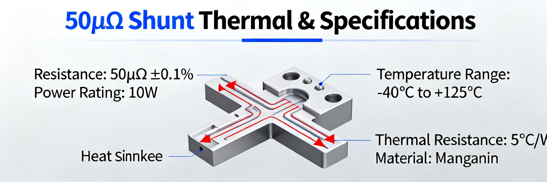
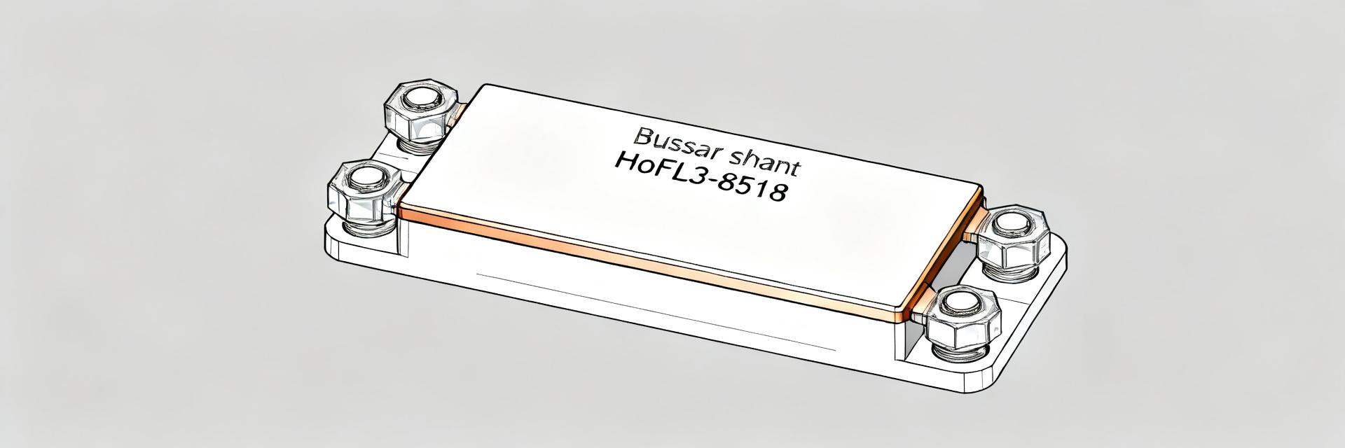
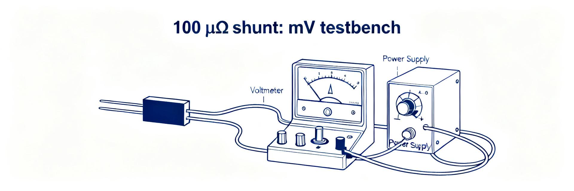
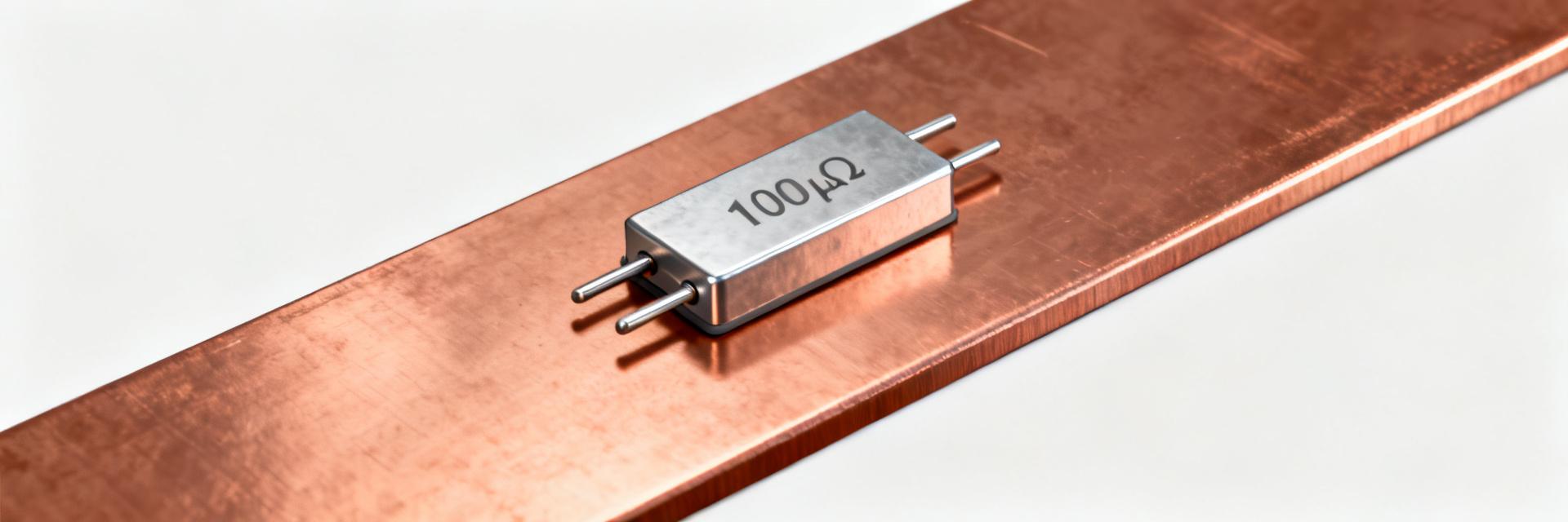
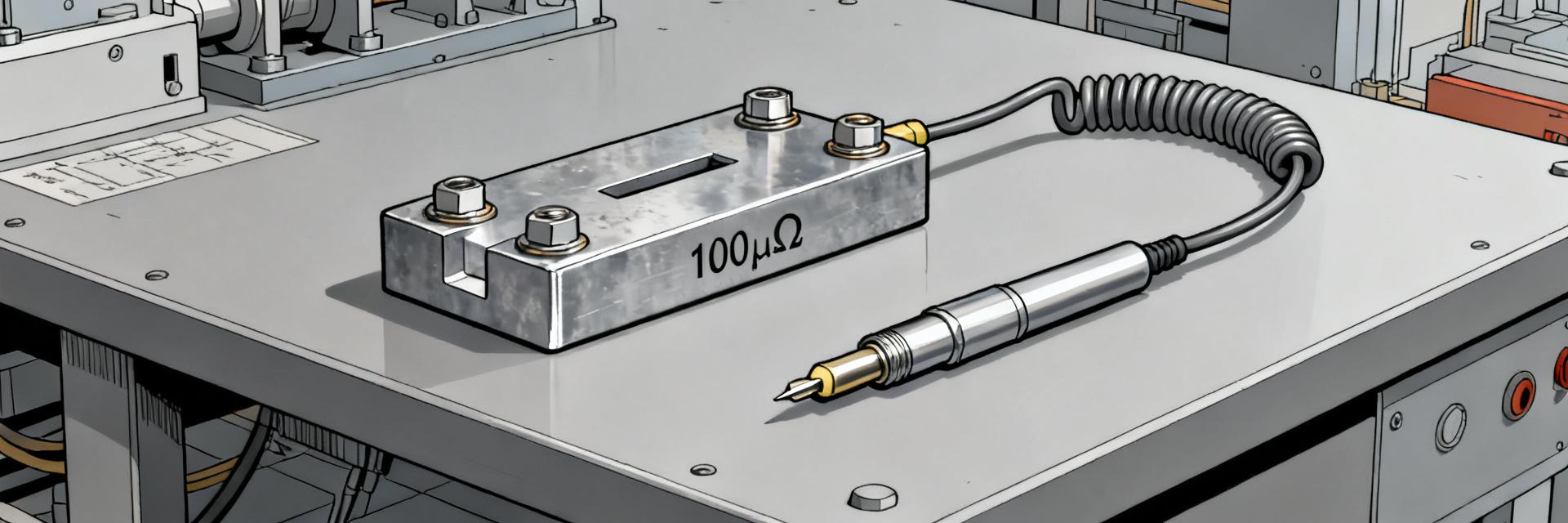
Measured baseline: 50 µΩ nominal with typical ±0.5–1% tolerance; continuous dissipation approaches tens of watts at high currents, and continuous losses can enter the 24–30 W range as current rises — understanding thermal behavior is critical for reliable current sensing. This article consolidates electrical specifications, explains a repeatable thermal test methodology, and interprets thermal test results so engineers can size ADC front-ends and set safe continuous-current limits for the HoFL3-6918-A. 1 — Product overview & key specs (background) 1.1 Mechanical & mounting details The HoFL3-6918-A arrives as a compact metal-alloy shunt optimized for busbar or screw-mount integration; typical dimensions are length ~69 mm, width ~18 mm, thickness ~6 mm with a mounting pitch that matches M5 screw fixtures. Recommended screw torque is 2.5–4.0 N·m to ensure low contact resistance; mass is typically under 40 g. On receipt, inspect for visible deformation, verify continuity and nominal resistance, and confirm mating hardware fits the suggested PCB/chassis footprint for best thermal path. 1.2 Electrical baseline: resistance, tolerance, TCR Nominal resistance: 50 µΩ. Typical tolerance grades offered: 0.5% and 1.0%. Temperature coefficient of resistance (TCR) commonly ranges from +50 to +150 ppm/°C depending on alloy and batch. Quick datasheet-style reference follows; use V = I·R to verify voltage drop at rated currents. ParameterValue Nominal R50 µΩ Tolerance0.5% / 1% TCR~50–150 ppm/°C Voltage drop @700 A35 mV (V = I·R) Terminal A Screw Mount M5 Manganin Alloy Element 50 µΩ Nominal Terminal B Screw Mount M5 Sense A (V+) Sense B (V-) I_in I_out 2 — Electrical performance & sizing calculations (data analysis) 2.1 Voltage drop, ADC sizing & measurement considerations Voltage drop examples using V = I·R: 100 A → 5.0 mV, 300 A → 15.0 mV, 700 A → 35.0 mV. For a 50 µΩ shunt these drops require low-noise amplification; target a sense amplifier gain that places full-scale ADC input near mid-to-high range while preserving headroom for transients. Example: with a 12-bit ADC and 100 mV full-scale input, a gain of ~3 gives 35 mV×3 = 105 mV, near full-scale; a 16-bit ADC with gain 10 yields ~350 mV full-scale for high resolution and noise margin. 2.2 Power dissipation & thermal loading calculations Power dissipation follows P = I^2·R. Examples: 100 A → 0.5 W, 300 A → 4.5 W, 700 A → 24.5 W. Continuous vs peak: continuous ratings must account for chassis conduction and convection; short pulses can tolerate higher instantaneous P but require thermal recovery time. Use the power table below to estimate generated heat and to plan cooling and derating. Current (A)Power (W) 1000.5 3004.5 70024.5 3 — Thermal testing methodology (method guide) 3.1 Lab setup, instrumentation & mounting for repeatable tests Recommended instruments: programmable DC source or electronic load capable of target currents, calibrated thermocouples (Type K) or RTDs attached with low-thermal-resistance adhesive, an infrared camera for spatial profiling, and a data logger for continuous acquisition. Mount shunt using the specified torque, ensure clean, flat contact surfaces, and document the thermal interface materials and fixture geometry; measure at three points: shunt body, adjacent PCB (if present), and ambient to derive thermal gradients and thermal resistance. 3.2 Test profiles, durations & safety protocols Run steady-state ramps (increase current in steps until thermal equilibrium), transient pulses (5 s, 30 s, 60 s) and overload pulses with controlled duty cycles. Stabilization criterion: ΔT < 0.5 °C over 5 minutes indicates steady state. Safety: always enclose test setup, use current-limited sources or fast fusing, and implement thermal cut-offs to prevent catastrophic heating during a failed mount or shorted measurement lead. Record ambient and airflow conditions for repeatability of the thermal test. 4 — Thermal test results & interpretation (case/data) 4.1 Typical steady-state temperature rise vs current (how to present/findings) Plot temperature rise (°C above ambient) versus RMS current and extract thermal resistance Rth = ΔT / P (°C/W). Present both tabular data and a chart to show linearity and any knee points where conduction dominates. Key metrics: Rth-to-ambient, shift in resistance with temperature, and maximum continuous current at target ambient (e.g., 25 °C). Use these metrics to convert measured ΔT thresholds into safe continuous-current ratings for system design. 4.2 Transient heating, cooldown behavior & failure modes Transient curves reveal time constants and peak overshoots during pulses; a long cooldown or continuing resistance drift after cooling often points to poor thermal contact or elevated contact resistance. If the measured resistance drifts beyond specified tolerance after heating, re-inspect mounting faces, retorque hardware, and repeat thermal test; persistent drift may indicate material change or damage. Archive thermal test data for QA and regression checks. 5 — Integration, selection & application checklist (actionable recommendations) 5.1 Mounting, cooling & derating strategies Best practice: bond the shunt to a heat-spreading plate or chassis using high-contact-pressure fasteners and, if applicable, thermal interface material on mating surfaces. For forced convection, specify airflow and measure ΔT under expected flow. Rule of thumb for derating: reduce continuous current by ~5% for each 10 °C above 25 °C ambient; verify with system-level thermal tests that include enclosure effects. 5.2 Measurement best practices, calibration & QA steps Before deployment perform zero-offset calibration, temperature drift characterization, and an in-situ verification under a known load. Procurement checklist: select the required tolerance grade, specify TCR, request milliohm-level test certificates, and confirm mounting hardware matches recommended torque. Implement periodic drift tests in maintenance schedules and log calibration records for traceability. Summary / Conclusion (10–15% of article) For reliable high-current sensing, the HoFL3-6918-A requires attention to mounting and thermal management; ADC sizing and continuous-current limits should be driven by measured power dissipation and thermal-test-derived Rth. Run controlled thermal test profiles, document stabilization criteria, and use the derived thermal resistance to create system derating curves. Use V = I·R and P = I^2·R as the foundational calculations when integrating the HoFL3-6918-A into measurement systems. HoFL3-6918-A is 50 µΩ nominal with 0.5%–1% tolerance and modest TCR; verify on arrival and confirm torque for low contact resistance. Voltage drops: 100 A → 5 mV, 300 A → 15 mV, 700 A → 35 mV; amplifier gain and ADC resolution must reflect these small signals. Power dissipation scales as I^2·R; expect ~24.5 W at 700 A and plan chassis conduction or forced convection accordingly. Thermal test methodology and recorded thermal test data determine safe continuous-current derating for your enclosure and ambient. Frequently Asked Questions Q: What is the nominal resistance and tolerance of the HoFL3-6918-A? The nominal resistance is 50 µΩ with common tolerance grades of 0.5% and 1.0%. Confirm batch certificates and measure resistance on arrival at room temperature to validate. Q: How should I size the ADC for a 50 µΩ shunt at high currents? Calculate V = I·R for expected currents, choose amplifier gain to place that voltage near ADC full-scale while leaving headroom for transients; for example, a 16-bit ADC with gain 10 provides good resolution for 35 mV nominal drops at 700 A. Q: What thermal test profile is recommended? Combine steady-state ramps to equilibrium with short-duration pulses (5–60 s) and monitor ΔT until stabilization criteria (ΔT < 0.5 °C over 5 min) are met. Record ambient, airflow, and mounting torque for reproducibility and safety. Q: How should I manage heat dissipation and derate the HoFL3-6918-A at high temperatures? Bond the shunt to a heat-spreading plate or chassis using high-contact-pressure fasteners and thermal interface material (TIM). For derating, reduce continuous current by approximately 5% for every 10 °C rise above 25 °C ambient, verifying limits with system-level thermal tests.